Characterizing Long Term Board Level Strain Coupling and Mold Compound Creep Kinetics in High Precision Surface Mount Sensor Assemblies
Characterize mold compound viscoelastic relaxation and decouple board strain through routing slots to prevent unrecoverable long-term sensor calibration drift.


Anchor
Surface mount precision sensors register mechanical deformations originating meters away from the silicon die. When an assembly solders a quad-flat no-leads (QFN) or land grid array (LGA) package directly to an FR4 circuit board, the package turns into a structural element of the host substrate. The printed circuit board expands, contracts, warps, and absorbs moisture.
Solder joints transmit these macroscopic board strains into the encapsulated sensor package, where epoxy mold compound (EMC) transfers the resulting stress directly into the microelectromechanical systems (MEMS) diaphragm, piezoresistive bridge, or capacitive sensing cell. The initial factory calibration certificate records a zero-point balance captured under zero external load at 25 degrees Celsius. Solder reflow induces plastic deformation in the intermetallic joint, followed by cooling contractions that lock in parasitic assembly strains exceeding 600 microstrain across the sensing element.
The sensor zero point shifts immediately following board mounting. Factory-trimmed accuracy claims of 0.05 percent full-scale wander by an order of magnitude within hours of reflow cooling. This initial mechanical offset decays through post-assembly relaxation, yet the relaxation curve is neither rapid nor monotonic.
The epoxy mold compound undergoes secondary chemical post-curing, enthalpy relaxation, and physical aging, creating an active viscoelastic medium that translates host board flexure into time-dependent sensor drift. Buyers evaluating precision sensors for three-to-ten-year operating windows discover that long-term accuracy depends less on the silicon design than on the viscoelastic relaxation rate of the mold compound surrounding it.
IPC-7095 Class 3 voids beneath central thermal ground pads amplify board-to-die mechanical coupling gradients across multi-axis MEMS strain cells.
Long-term field stability decouples from initial component specifications when board strains couple mechanically to package encapsulants. An uncapped thermal stress or humidity-induced board warp continuously re-biases the internal strain state of the die. Metrology personnel attempting to verify field performance find that removing external board constraints returns the sensor toward its baseline value, proving that the drift originated outside the silicon.
Resolving this packaging interaction requires characterizing the mechanical load paths, measuring the constitutive relaxation kinetics of the polymeric matrix, and calculating the true metrological uncertainty introduced by the circuit board assembly.
Substrate thickness, trace distribution, solder alloy selection, and mold compound glass transition temperature govern the mechanical transfer function. An unverified assembly running standard SAC305 lead-free solder experiences continuous creep at room temperature, while the mold compound relaxes its locked-in reflow stresses over months of field deployment. Sourcing contracts that omit package-to-board mechanical isolation clauses transfer the financial responsibility for unrecoverable calibration drift entirely onto the buyer.


Pathway
The transmission of structural strain from a printed circuit board into a microscopic sensing element follows a defined structural chain. The printed wiring board functions as an anisotropic mechanical beam with an in-plane elastic modulus varying between 18 and 26 gigapascals depending on internal copper distribution. Under operational thermal cycling between minus 40 and plus 85 degrees Celsius, the glass-reinforced epoxy substrate expands with a coefficient of thermal expansion (CTE) of 14 to 17 parts per million per Kelvin in the in-plane axes, and 50 to 70 parts per million per Kelvin in the through-thickness axis.
The packaged silicon die exhibits a rigid CTE of 2.6 parts per million per Kelvin and an elastic modulus of 130 to 170 gigapascals depending on crystallographic orientation.

Mechanical Strain Transmission across Packaging Interfaces
Solder interconnects absorb the direct displacement mismatch between the substrate and package landing pads. In high-density assemblies utilizing SAC305 solder (96.5 percent tin, 3.0 percent silver, 0.5 percent copper), the joint operates at a homologous temperature above 0.6 even at ambient room conditions. The solder yields plastically during the cool-down phase of reflow soldering, retaining high residual shear stresses.
As the host board warps due to asymmetric layer stacking, uneven component distribution, or external mounting torque, the solder joints impose bending moments on the package substrate or leadframe.
The epoxy mold compound encapsulates the silicon die and copper leadframe, forming a solid composite matrix filled 70 to 90 percent by weight with fused silica particles. The encapsulant exhibits an elastic modulus of 15 to 28 gigapascals below its glass transition temperature and acts as a mechanical stress transmitter. Board strains transmitted through solder joints travel into the package leads, propagate into the mold compound matrix, and load the active face of the silicon through the die attach interface and the direct EMC contact surfaces.
Piezoresistive stress sensors integrated on test dice confirm that board-level four-point bending loads transmit between 12 and 35 percent of host substrate surface strain directly to the active silicon surface, with the precise ratio governed by package geometry and die pad thickness.
| Interface Layer | Elastic Modulus (GPa) | CTE Below Tg (ppm/K) | Tg Range (°C) | Strain Transmission Efficiency (%) |
|---|---|---|---|---|
| FR4 Substrate (In-Plane) | 22.0 ± 3.0 | 15.0 ± 1.5 | 140 to 175 | 100 (Reference Driver) |
| SAC305 Solder Joint | 42.0 ± 4.0 | 21.5 ± 1.0 | N/A (Melts 217) | 65 to 85 (Plastic Dependent) |
| Silica-Filled Mold Compound | 24.0 ± 2.5 | 8.5 ± 1.0 | 120 to 160 | 35 to 55 |
| Epoxy Die Attach Adhesive | 6.5 ± 1.5 | 35.0 ± 5.0 | 65 to 110 | 15 to 30 |
| Silicon Die (P-Type 100) | 169.0 ± 5.0 | 2.6 ± 0.2 | N/A | 12 to 35 (Coupled Strain) |
The transmission efficiency drops when low-modulus die-attach adhesives absorb displacement before energy reaches the die. Silicon sensor dies attached using soft silicone materials with moduli below 10 megapascals isolate shear loads effectively. High-reliability industrial sensors use filled epoxy formulations to pass standard thermal shock and automotive drop tests, sacrificing mechanical isolation for adhesion and fatigue resistance.
This stiffness forces the assembly to transmit environmental board warping directly into the active sensor elements.
Piezoresistive coefficients within monocrystalline silicon convert these transmitted stresses into electronic voltage offsets. A differential pressure sensor or precision piezoresistive strain gauge reads mechanical strain as an apparent pressure or force change. In capacitive pressure sensors, package stresses deform the silicon substrate beneath the cavity anchor points, tilting capacitor electrodes and altering rest capacitance.
These shifts mimic physical signal inputs, introducing baseline calibration errors indistinguishable from true process variation.
A supplier will state that solder pad layouts strictly follow IPC-7351 recommendations and therefore board strains remain within standard manufacturing margins.


Relaxation
Thermosetting epoxy mold compounds are cross-linked amorphous networks that operate below their glass transition temperature during standard industrial sensor operation. Despite operating in the glassy state, these polymer networks exhibit significant viscoelasticity. When subjected to constant strain from post-reflow solder warpage or chassis mounting fasteners, the stress within the mold compound decays continuously through molecular relaxation processes.
Conversely, sustained operational board stresses induce viscoelastic and viscoplastic creep strains across the polymer chains, shifting the load distribution over time.

Kinetics of Time-Dependent Mold Compound Relaxation
Viscoelastic relaxation in highly filled mold compounds follows the time-temperature superposition principle. Polymer chains undergo cooperative segmental rearrangements at rates dictated by their free volume. The mechanical relaxation modulus over extended time frames follows the Kohlrausch-Williams-Watts (KWW) stretched exponential model or multi-element generalized Maxwell models.
The time-dependent relaxation modulus E(t) takes the following constitutive mathematical form:
E(t) = E_infinity + (E_0 – E_infinity) exp(-(t / tau)^beta)
In this relationship, E_0 represents the instantaneous glassy modulus, E_infinity is the long-term equilibrium modulus, tau is the characteristic relaxation time constant, and beta is the non-exponential stretching parameter bounded between 0.35 and 0.65 for silica-filled industrial packaging resins. Dynamic mechanical analysis (DMA) shows that characteristic relaxation times range from hundreds of hours at 25 degrees Celsius to tens of hours at 85 degrees Celsius.
Viscoelastic relaxation rates inside silica-filled novolac compounds accelerate tenfold for every twenty-degree elevation toward the resin glass transition temperature.
Physical aging alters these relaxation kinetics. After cooling from the 260-degree reflow peak, the epoxy resin enters a non-equilibrium glassy state containing excess free volume. As the assembly resides at room temperature, polymer chains collapse toward their thermodynamic equilibrium state, decreasing the molecular free volume.
This aging process increases the material density, elevates the effective instantaneous modulus, and shifts the relaxation spectrum toward longer time constants. A sensor left in storage exhibits a moving baseline because the mold compound physical state evolves independently of external inputs.
Equilibrium shifts faster when sensors operate in elevated ambient conditions. Moisture absorption introduces plasticization kinetics that disrupt inter-chain hydrogen bonds, lowering the glass transition temperature by 15 to 30 degrees Celsius and depressing the instantaneous relaxation modulus. A sensor calibrated in a dry factory environment experiences accelerated viscoelastic relaxation once ambient moisture penetrates the package envelope, fundamentally altering the mechanical transfer function between the circuit board and the sensing element.
Uncalibrated baseline drift exceeding one microvolt per volt per thousand hours occurs in unbaked assemblies deployed directly into industrial monitoring enclosures.


Shift
Piezoresistive sensing matrices convert assembly-level viscoelastic relaxation directly into electrical parameter drift. In bulk silicon, mechanical stress alters carrier mobility through the piezoresistive effect. The fractional change in electrical resistivity links to principal package stresses through the longitudinal and transverse piezoresistive coefficients.
For p-type silicon elements oriented along the direction of a (100) silicon wafer, the piezoresistive stress components parallel and orthogonal to current flow dictate zero-load offset shifts.

Electromechanical Transduction of Creep Stresses
As the mold compound creeps under continuous post-assembly stress, the balance of internal forces across the die surface reorganizes. Initial post-soldering stress distributions concentrate high compressive forces at die corners, while the active sensing membrane in the center experiences biaxial compression ranging from 40 to 90 megapascals. Viscoelastic relaxation reduces these peak stresses over time while evening out localized spatial gradients.
A piezoresistive Wheatstone bridge balanced during initial factory testing with balanced arm resistances drifts out of symmetry as the localized stress beneath individual resistors shifts at unequal rates.
Capacitive MEMS structures experience different electrical consequences from the same mechanical source. In surface-micromachined accelerometers and capacitive absolute pressure sensors, the silicon die attaches to a central paddle or substrate land. Mold compound relaxation applies an asymmetric bending moment to the package perimeter, warping the die substrate.
This warpage tilts internal proof masses and deforms capacitive sense gaps that measure less than two micrometers in width. A board warp of three micrometers across a package diagonal alters the quiescent capacitance by femtofarads, causing substantial baseline drift that appears on digital sensor registers as uncommanded output wander.
- Piezoresistive bridge unbalance develops when differential relaxation rates across orthogonal resistor arms alter zero-load offset voltages by hundreds of nanovolts.
- Proof mass tilt distortion in capacitive accelerometers induces false DC acceleration signals through asymmetric sensing electrode spacing changes.
- Membrane perimeter buckling in absolute pressure sensors alters cavity volume and shifts diaphragm mechanical stiffness.
- Thermal coefficient alteration occurs as relaxation-induced residual stresses modulate the intrinsic silicon bandgap and carrier concentration profiles.
Long-term offset drift measurements collected over 5,000 hours reveal distinct stages. The initial 500 hours exhibit rapid drift dominated by solder creep and the initial relaxation of high-magnitude reflow stresses. Between 500 and 2,500 hours, the drift rate transitions into a logarithmic decay regime driven by primary viscoelastic relaxation within the bulk mold compound.
Beyond 2,500 hours, physical aging of the polymer and ambient cyclic moisture sorption dominate the drift profile, producing seasonal baseline shifts that simple linear factory calibration algorithms fail to predict.
A manufacturing assembly line will document total field failure rates below 50 parts per million when components remain within gross operational limits, yet half of those functional sensors operate well outside their advertised measurement accuracy grade.


Assay
Accurate quantification of board-level strain coupling requires physical instrumentation capable of isolating thermal expansion from viscoelastic deformation. Standard surface-mount strain gauges mounted directly to printed circuit boards provide verification of macroscopic substrate bending. Triaxial rosette gauges positioned adjacent to the sensor package measure the complete in-plane strain tensor, providing principal strains and orientation angles.
However, board-mounted gauges cannot measure the internal stress state of the encapsulated silicon die.

Experimental Methods for Internal Package Strain Isolation
Internal stress isolation relies on custom piezoresistive stress test chips, high-resolution moiré interferometry, or synchrotron micro-diffraction. Piezoresistive stress test chips contain arrays of rosettes consisting of four-terminal or serpentine diffused resistors optimized for stress extraction. These test assemblies map the complete surface stress distribution across the die before molding, after post-mold cure, following solder reflow, and during accelerated aging profiles.
Digital image correlation (DIC) applied to cross-sectioned assemblies tracks internal interface displacements under controlled thermal and mechanical loading cycles.
ASTM E831 thermomechanical analysis reveals that under-cured mold compound matrices undergo glass transition depression up to twelve degrees under operational storage environments.
Dynamic mechanical analysis (DMA) provides the constitutive viscoelastic parameters required for numerical simulation. Testing follows rigorous environmental profiles to capture both temperature-dependent and time-dependent behaviors:
- Mount rectangular bar specimens of cured mold compound inside a dual-cantilever DMA fixture.
- Apply an oscillatory strain within the linear viscoelastic region at a constant frequency of 1.0 hertz while ramping temperature from minus 50 to 200 degrees Celsius at 2.0 degrees per minute.
- Conduct frequency sweeps from 0.01 to 100 hertz across isothermal steps spaced at five-degree intervals between operating limits to construct master relaxation curves.
- Calculate shift factors using the Williams-Landel-Ferry (WLF) relation above glass transition and Arrhenius kinetics below glass transition.
Finite element analysis (FEA) incorporates these viscoelastic constitutive formulations to predict sensor offset shifts over multi-year deployments. Standard elastic models fail to predict long-term drift because they assume residual reflow stresses remain invariant over time. By implementing Prony series parameterizations of the relaxation modulus inside nonlinear mechanics solvers, analysts calculate the evolution of interfacial shear stress at the silicon-to-EMC boundary, capturing the decay of peak stresses and the gradual redistribution of strain toward sensing membranes.
| Maxwell Element (i) | Relaxation Time Tau_i (Hours) at 25°C | Normalized Modulus E_i / E_0 | Dominant Kinetic Regime |
|---|---|---|---|
| 1 | 0.85 ± 0.10 | 0.142 | Fast localized free-volume collapse |
| 2 | 12.4 ± 1.5 | 0.215 | Secondary chain segmental relaxation |
| 3 | 180.0 ± 20.0 | 0.288 | Primary backbone cooperative diffusion |
| 4 | 2,450.0 ± 250.0 | 0.190 | Long-range macromolecular reorientation |
| Equilibrium (Infinity) | Infinite | 0.165 | Fully cross-linked network baseline |
The parameter fit demonstrates that more than 60 percent of the total relaxation potential occurs over time scales exceeding 100 hours at ambient room temperature. Test protocols that assess sensor zero-point drift over standard 96-hour burn-in cycles capture less than half of the relaxation window, releasing parts into active inventory before the mechanical system enters its predictable logarithmic drift regime.
If the testing laboratory neglects humidity preconditioning during DMA coupon extraction, the measured glass transition temperature reads artificially high by ten to fifteen degrees, skewing the predicted multi-year drift models.


Isolation
Mitigating board strain coupling requires architectural changes across the board layout, package selection, and mechanical mounting topology. The primary mechanical objective involves breaking the structural continuity between the high-expansion host circuit board and the rigid, stress-sensitive silicon die. Relying on software calibration to eliminate board strain drift is inadequate because viscoelastic relaxation kinetics are nonlinear, path-dependent, and heavily modulated by variable environmental humidity profiles.
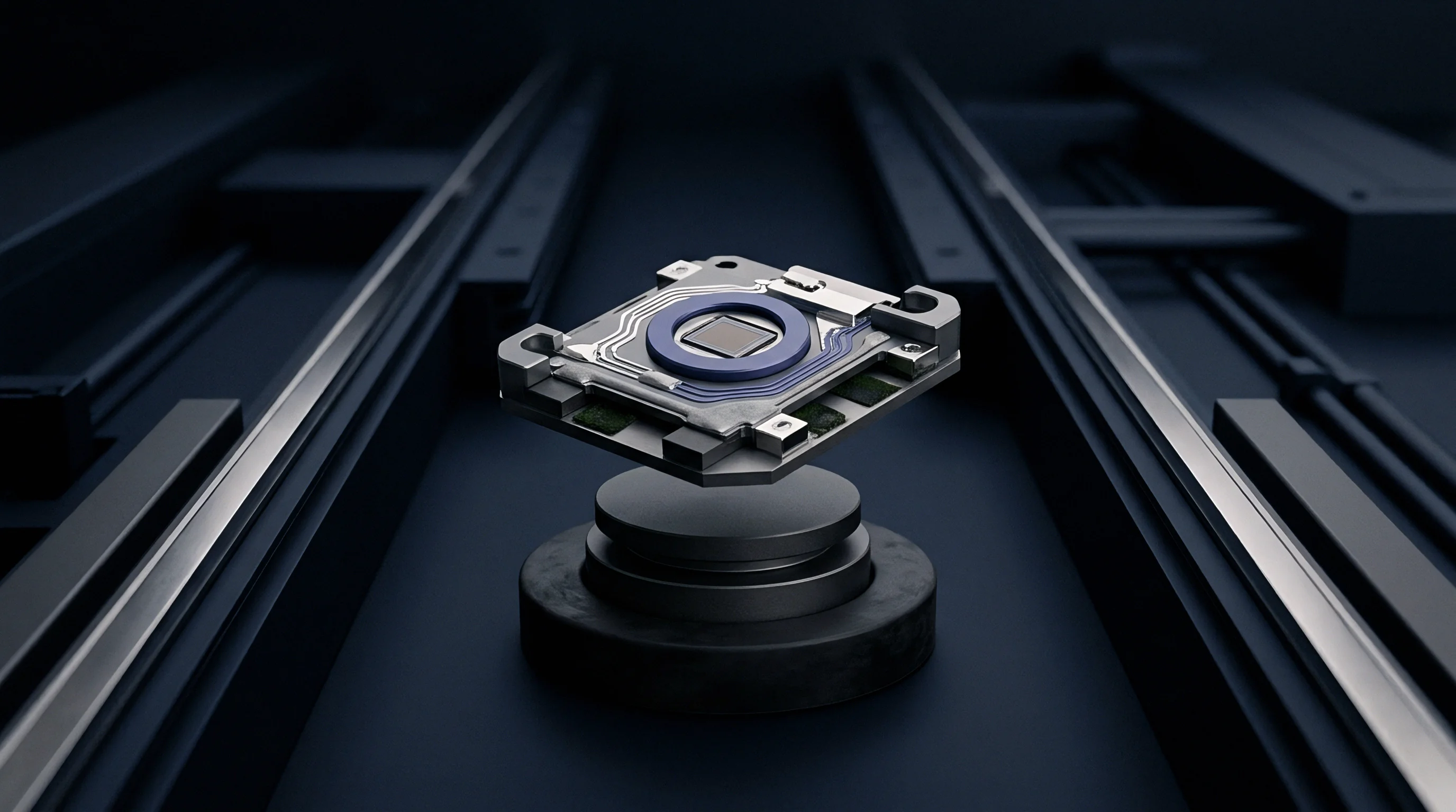
Substrate and Structural Decoupling Configurations
Physical isolation begins with the host printed circuit board layout. Integrating routing relief slots around precision sensor footprints mechanically decouples the package lands from structural board flexure. Milling U-shaped or cross-pattern isolation slots around a sensor creates a cantilevered or bridge-supported peninsula, reducing strain transmission from external board bending by 70 to 85 percent.
Locating mounting screw holes within 25 millimeters of a precision sensor introduces significant assembly torque stress, and this mounting pattern should be avoided.
Trace geometry and copper balance also dictate localized board warpage. Asymmetric copper distribution between the top and bottom layers beneath a sensor footprint induces localized bimetallic thermal bending during normal operating temperature swings. Placing a solid copper plane directly beneath a package land pattern while allowing sparse signal routing on opposing layers creates a localized thermal bending couple that directly flexes the sensor solder joints.
- Mechanical relief slots milled into the host printed circuit board interrupt the transmission of macroscopic flexural strains to the sensor landing zone.
- Symmetrical copper balancing across internal substrate layers prevents asymmetric bimetallic thermal warpage underneath the package footprint.
- High-standoff compliant interconnects such as gull-wing leads replace bottom-terminated land grid arrays to absorb lateral displacement mismatches through lead flexing.
- Corner-gluing or selective underfill must be analyzed carefully because rigid underfill materials increase package-to-board coupling by eliminating solder joint compliance.
Package architecture dictates internal isolation performance. Gull-wing leaded packages like the small outline package (SOP) or thin shrink small outline package (TSSOP) provide mechanical compliance through exposed lead geometry. The flexible copper leads absorb board-level differential expansion, reducing the strain transmitted to the die attach paddle to under five percent of total substrate strain.
For applications driven by spatial constraints to QFN or LGA packages, manufacturers must select packaging configurations incorporating soft die-attach materials or suspended silicon structures with micro-machined isolation frames.
Where high reliability requires bottom-terminated packages, post-reflow mechanical stabilization protocols become necessary. Thermal conditioning cycles held at 100 degrees Celsius for 48 hours immediately following surface mount assembly accelerate primary viscoelastic relaxation and physical aging. This thermal treatment forces the mold compound and solder joints past their initial high-drift kinetic regimes before final baseline calibration is performed on the fully assembled circuit board.
Does the integration of a compliant silicone die attach eliminate the requirement for board-level routing relief slots?
Silicone die attaches absorb shear displacement beneath the silicon base, yet mold compound encasing the active die face continues to transmit stress directly into sensitive microstructures. Structural relief slots on the host substrate remain necessary whenever operational zero-point tolerances are tighter than 0.1 percent of span.


Remedy
When mechanical decoupling cannot completely eliminate package stress, signal conditioning electronics and calibration methods must resolve residual baseline wander. Simple single-point zero adjustments conducted on newly manufactured boards capture an unstable mechanical transient. Sourcing agreements that do not define board-level mechanical preconditioning intervals accept shipments that will drift out of tolerance while sitting in warehouse packaging.

Metrological Verification and Calibration Architectures
System-level compensation relies on tracking external environmental factors that correlate with viscoelastic relaxation states. Temperature sensors integrated into the MEMS package provide thermal tracking, but standard polynomial temperature compensation cannot track path-dependent viscoelastic hysteresis. Integrating dedicated on-chip piezoresistive stress sensors adjacent to the active MEMS element allows direct measurement of the package stress tensor.
By reading these stress-monitoring bridges simultaneously with the primary sensing signal, internal digital signal processors apply real-time compensation algorithms that cancel the stress-induced baseline shift independent of time, temperature history, or board flexure.
For assemblies lacking dedicated stress-sensing hardware, factory burn-in must be budgeted based on true kinetic time constants. A worked uncertainty calculation highlights the operational risk. Consider a precision barometric pressure sensor with an advertised annual stability of ±0.1 hectopascal (equivalent to approximately 0.01 percent full scale).
Assume the package is an LGA format mounted with SAC305 solder to a 1.6-millimeter FR4 substrate, exhibiting an initial post-reflow assembly strain of 450 microstrain. If the mold compound possesses a typical relaxation amplitude of 20 percent over its first year at 25 degrees Celsius, the uncompensated mechanical shift generates a zero-point drift calculated through the assembly coupling factor:
Delta_Offset = Strain_Initial Relaxation_Fraction Coupling_Coefficient Sensitivity
Assuming a representative coupling coefficient of 0.22 and a piezoresistive transfer sensitivity of 0.003 hectopascal per microstrain:
Delta_Offset = 450 microstrain 0.20 0.22 0.003 hPa/microstrain = 0.0594 hectopascal
This single mechanical mechanism consumes nearly 60 percent of the total annual error budget, leaving minimal margin for silicon-level aging, power supply drift, or analog-to-digital converter reference instability. If the host board experiences an operational thermal excursion to 60 degrees Celsius, the relaxation rate accelerates by a factor of 4.2 based on Arrhenius scaling, driving the sensor completely outside its annual stability specification within the first four months of service.
Procurement teams must address this vulnerability through specific commercial acceptance criteria:
- Documented pre-conditioning bake schedules specifying minimum duration and temperature thresholds prior to final baseline zero-offset programming.
- Board mounting strain qualification dossiers detailing maximum permissible substrate flexure during assembly fastening, verified by rosette strain gauges.
- Humidity-induced zero-shift validation data tracking package behavior through 85 degrees Celsius and 85 percent relative humidity environmental exposures.
- Guaranteed annual stability boundaries that explicitly incorporate board-level solder reflow effects rather than standalone component test values.
Sourcing precision surface-mount sensors without verifying encapsulant viscoelastic properties leaves systems vulnerable to systemic field calibration drift that hardware replacements and field service updates can never fully resolve.
Contracts that specify sensor accuracy solely against unmounted component datasheets leave the buyer fully liable for all field returns caused by board-level mechanical coupling.