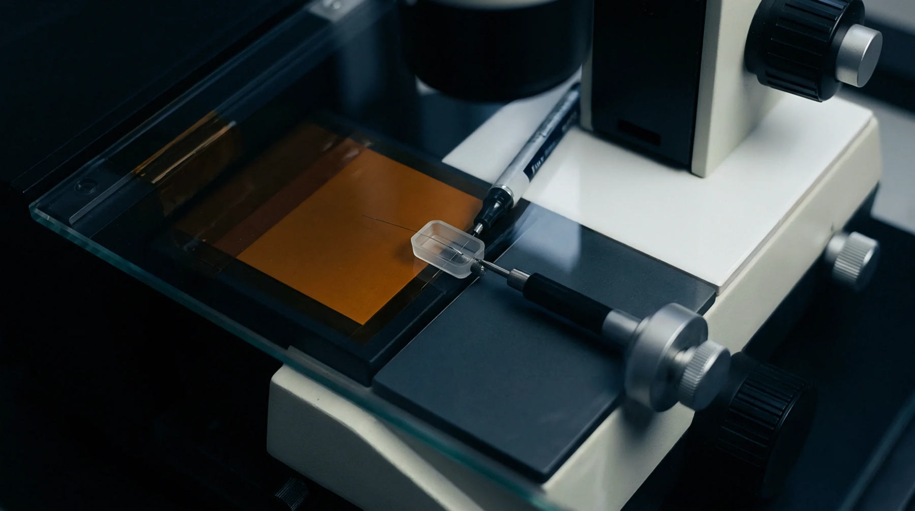
Molded Package Stress Effects on Piezoresistive and Capacitive Transducer Zero-Point Calibration
Transfer molding stresses deform transducer diaphragms, shifting zero-point calibration by up to three percent full scale across reflow assembly cycles.
Transfer molding stresses deform transducer diaphragms, shifting zero-point calibration by up to three percent full scale across reflow assembly cycles.

Constant current drive cancels piezoresistive span drift by exploiting positive bridge resistance growth to offset the negative temperature coefficient of sensitivity.

Viscoelastic die-attach relaxation shifts piezoresistive bridge zero-points; Prony-series modeling predicts and isolates this packaging strain drift.

High thermal sensitivity in silicon strain sensors stems from carrier mobility drop while permanent drift originates from thermally activated dislocation glide.

Packaging stress shifts silicon bandgap output voltages via piezoresistive and piezojunction mechanisms, requiring crystallographic layout and compliant packaging.

Polymer creep in sensor die-attach layers relaxes packaging pre-stress, causing continuous zero offset drift that requires low-creep adhesives or recalibration.

Silicon thermal expansion mismatch induces mechanical packaging stresses that drive piezoresistive offset drift, requiring compliant anchors or ceramic mounts.

Common centroid geometry eliminates linear gradients in precision silicon references, transferring residual drift limits entirely to packaging stress and bus trim.

Coupled thermodynamic drift modeling links secular resistance shifts to turnover decay, reducing long-term calibration uncertainty below 0.02 ppm.

Dynamic package shear stress produces non-inverting thermal hysteresis loops that defeat memoryless polynomial matrix compensation in multi-axis sensors.

Boron piezoresistive compensation balances positive resistance shifts against negative gauge factor decline via tailored current circuits or ASIC polynomials.

Ion implantation optimizes piezoresistive sensor sensitivity by balancing boron dose against gauge factor decay, junction depth, and thermal span stability.

Anodic bonded glass pedestals require aspect ratios above 1.25 and compliant submounts to decouple expansion shear strains from sensitive silicon diaphragms.

Packaging mold shrinkage and board reflow solder strain alter silicon bandgap voltages via piezoresistive coupling, demanding compliant leads or ceramic packages.
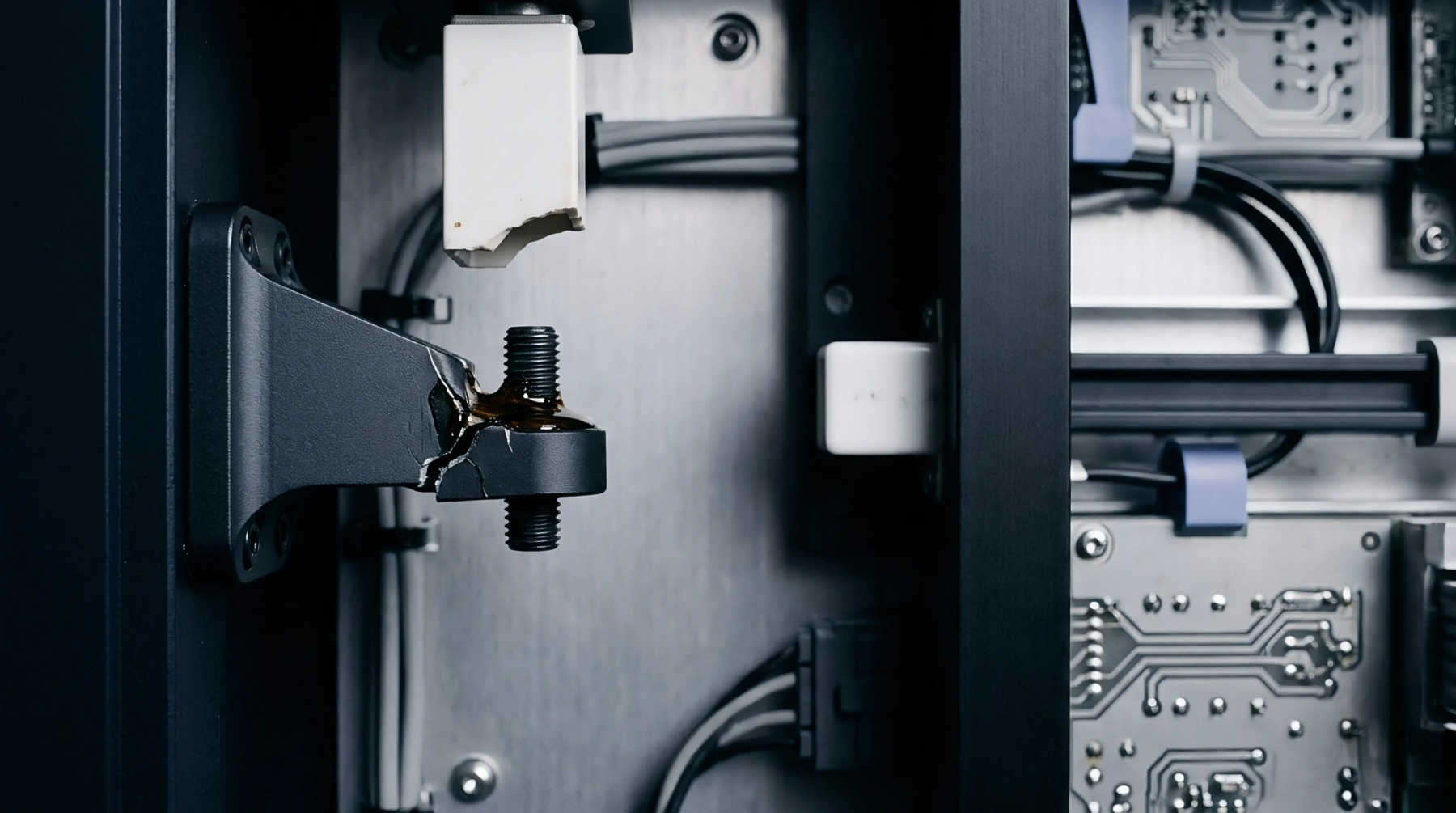
Calculate viscoelastic stress transfer by fitting multi-mode Prony series DMA data and applying Arrhenius-corrected shift factors under thermal cycling dwells.

Surface mount packaging transfers printed circuit board flexure to piezoresistive silicon dies, causing bridge zero shifts that defeat digital compensation.

Packaging stress relaxation drives non-linear zero drift in piezoresistive sensors, requiring early recalibration before shifting to extended intervals.
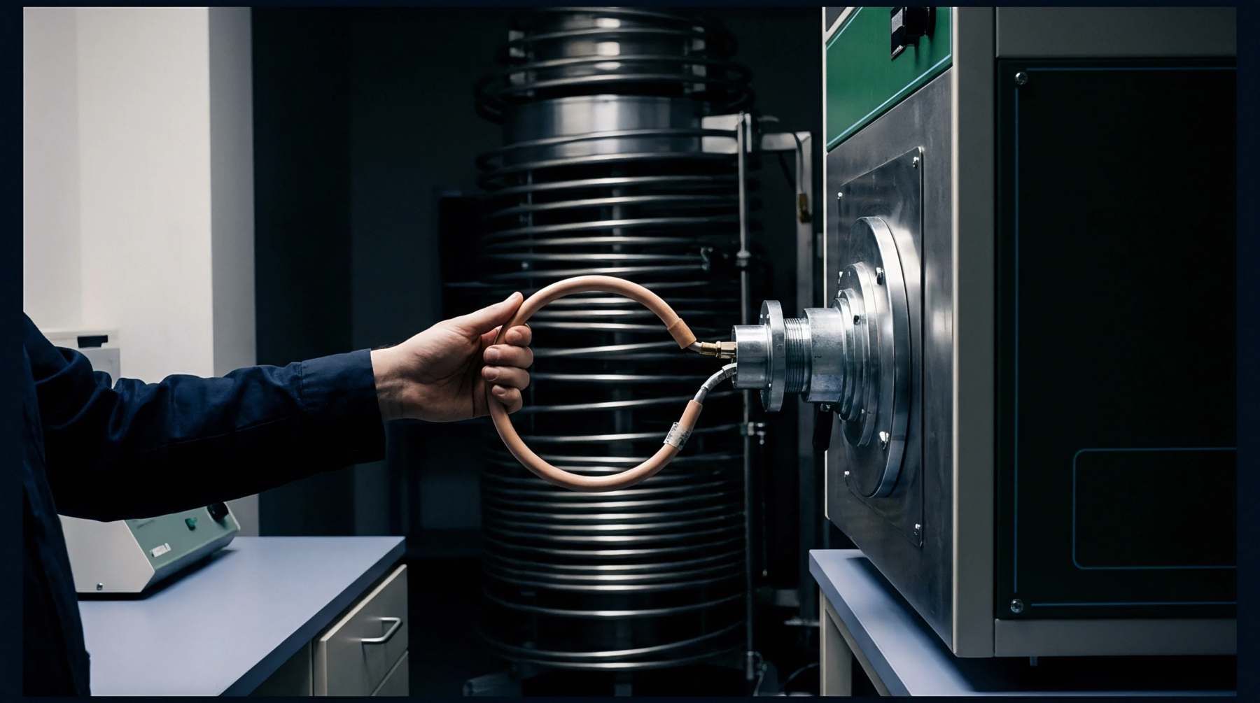
Water diffusion into silicon sensor passivations causes asymmetric swelling stress that drives zero point drift unless arrested by true hermetic packaging.

Substrate warpage injects mechanical strain directly into the sensing die, shifting analog front-end bridge balance past digital trim limits.
Precision voltage references demand symmetric copper lands, isolation slots, and convective shielding to suppress piezoresistive and thermoelectric drift.

Packaging thermal stress alters piezoresistive bridge balance; maintaining sensor accuracy requires etched isolation moats and cooling rates under 2 C per minute.
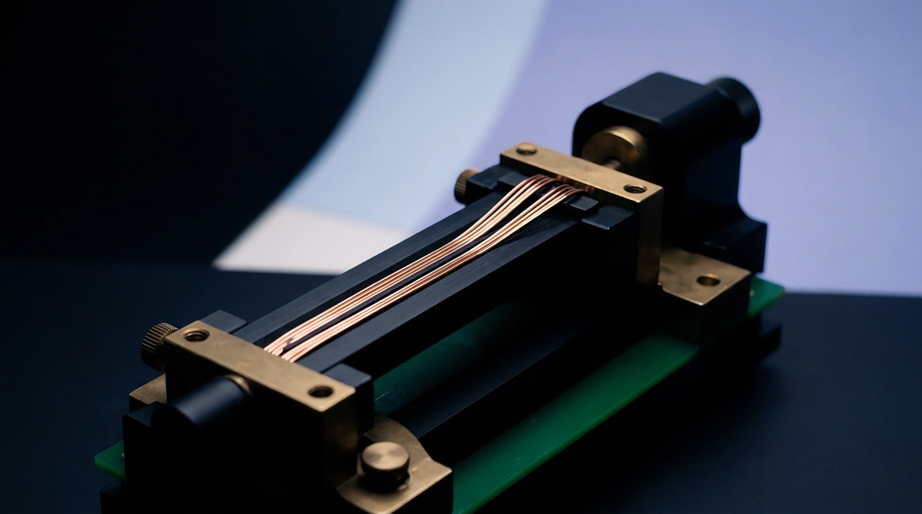
Piezoresistive diaphragm performance demands matching current excitation to silicon thermal coefficients and isolating media via low-volume oil cavities.

Proton displacement damage degrades piezoresistive sensitivity by generating lattice defects that reduce free carrier mobility and effective gauge factor.

Minimizing reference drift requires non-solder-mask-defined pads, compliant gull-wing packages, and perimeter routed slots to isolate circuit board strain.

Lead-free reflow generates high interfacial shear stresses across LGA pads, driving piezoresistive offset shifts that demand post-bake calibration routines.
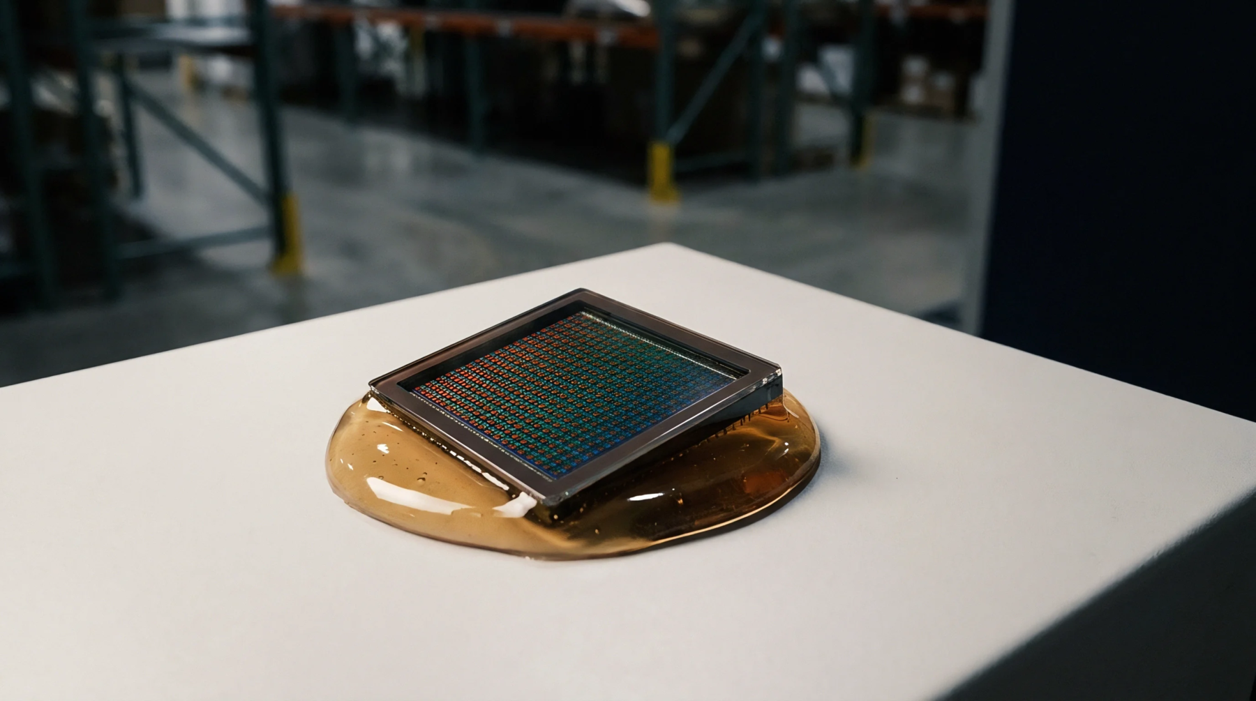
Viscoelastic adhesive relaxation in ceramic LCC packages causes time-dependent zero drift, requiring master-curve Prony modeling to quantify long-term offset shift.
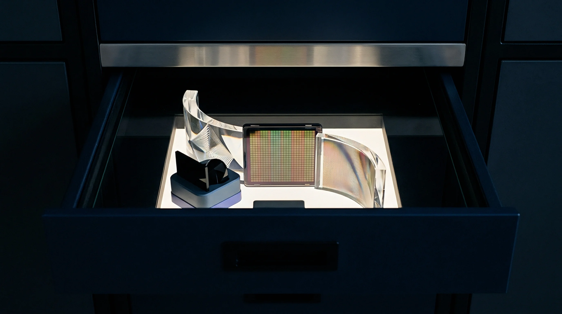
Polymeric die-attach relaxation causes time-dependent thermal strain hysteresis in silicon MEMS, producing zero-offset drift that static calibration cannot fix.

Silicon piezoresistors provide gauge factors exceeding one hundred but require mechanical isolation to decouple die stress from intrinsic thermal sensitivity.

Unpassivated wafer conversion packaging transfers mold compound reflow stresses directly into analog trim circuits, shifting factory register offsets.
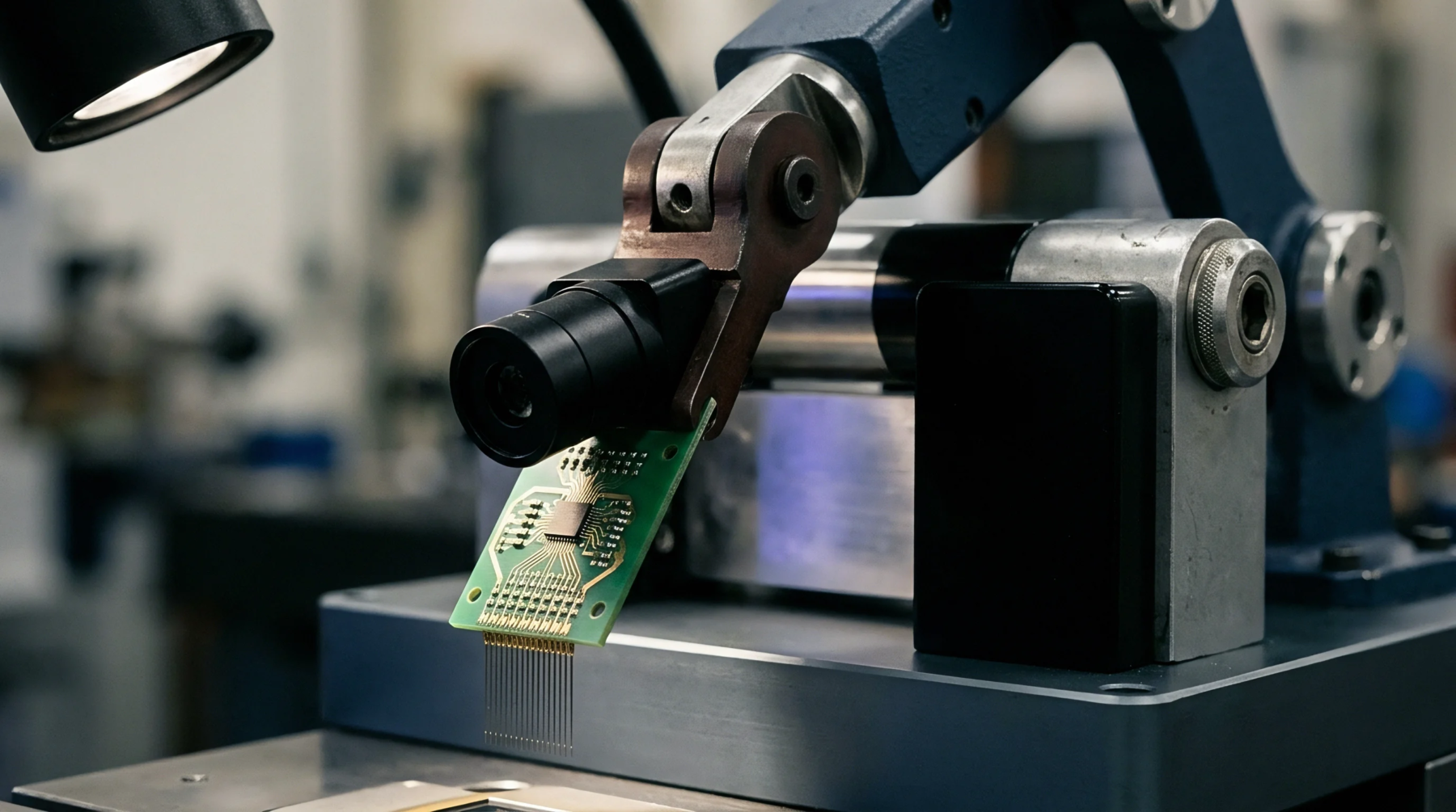
Characterize mold compound viscoelastic relaxation and decouple board strain through routing slots to prevent unrecoverable long-term sensor calibration drift.
Expertise is a utility, not a secret. sentiention™ publishes its working knowledge as open reference: intelligence layer covering the materials it sources, the markets it enters, and the reference that serves both.