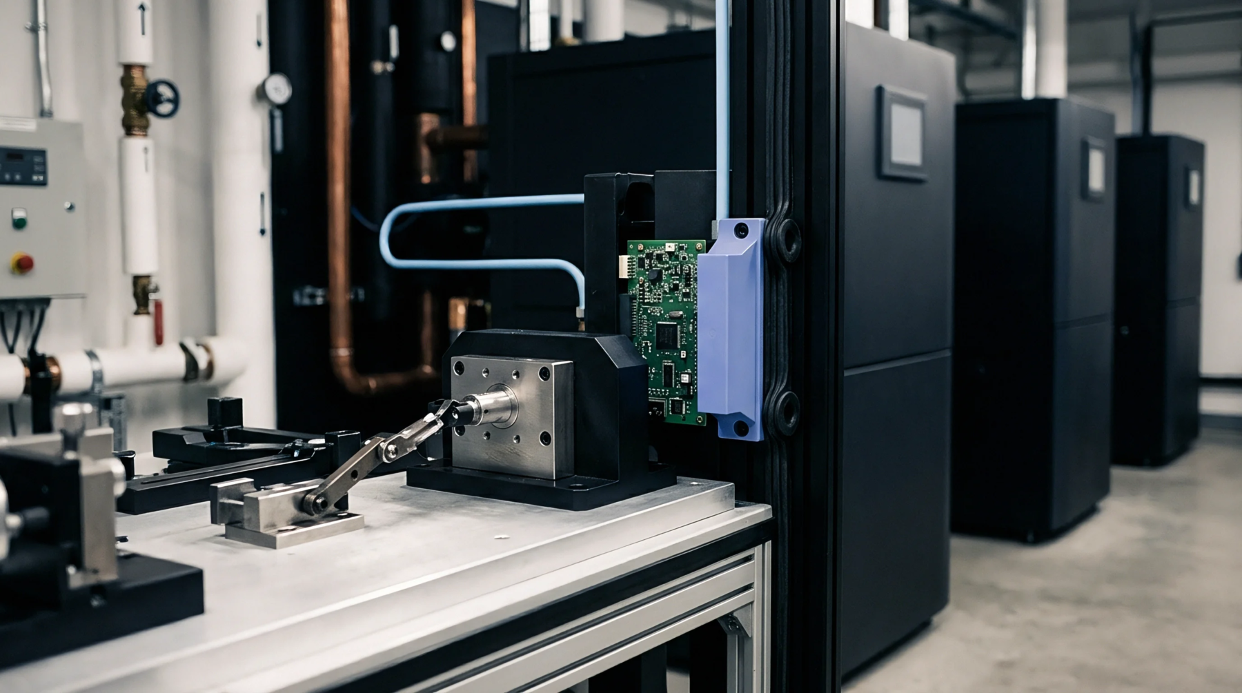
Board Flex Reaching the Die as Offset Error after Assembly
Board flexure transfers shear strain through solder joints into silicon dies, shifting zero-point offsets; isolate footprints using slots or diagonal placement.
Board flexure transfers shear strain through solder joints into silicon dies, shifting zero-point offsets; isolate footprints using slots or diagonal placement.
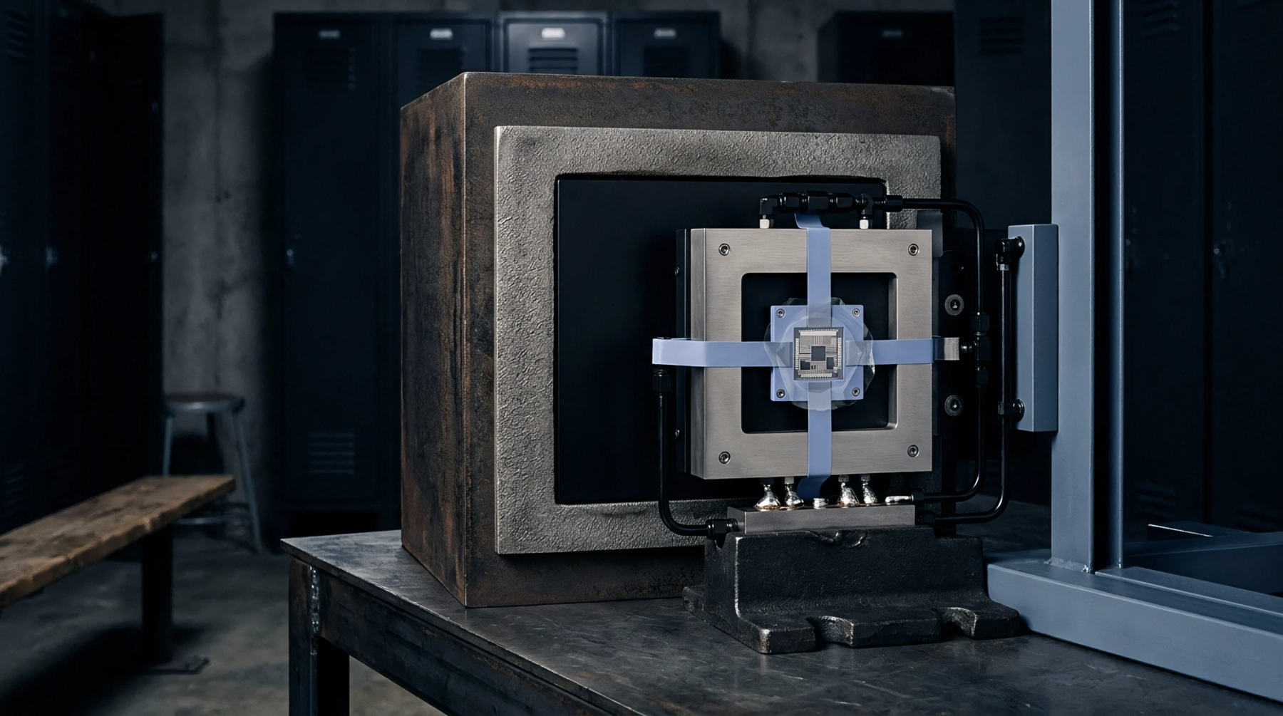
Polymer encapsulant swelling induces parasitic diaphragm stresses that drive zero-offset drift requiring hydrophobic materials or multi-variable digital compensation.
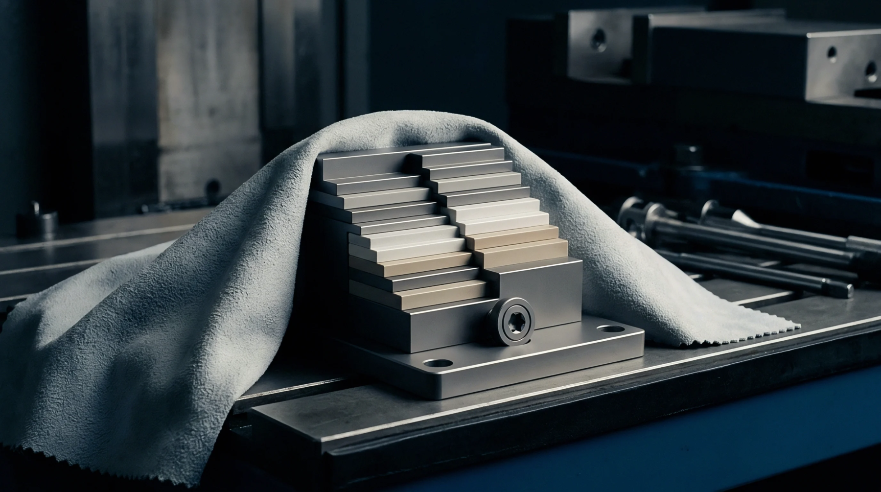
Optimal piezoresistive stability requires heavy surface boron doping above 2e19 cm-3 combined with plasma-activated silane coupling to prevent delamination.
P-type silicon piezoresistors doped with boron to 1e18 cm-3 achieve an optimal balance between gauge factor magnitude and thermal coefficient stability.

High-temperature package creep redistributes interfacial strain to drive long-term sensor drift, requiring viscoplastic modeling and burn-in stabilization.

Temperature cross-sensitivity in pressure sensors stems from physical die stress and semiconductor carrier shift, requiring digital ASIC polynomial compensation to control thermal error bands.
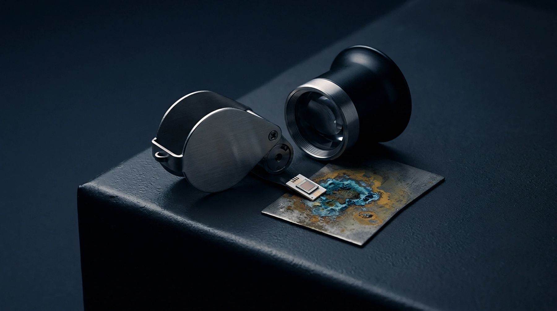
Silicon substrate thermal expansion alters MEMS structural spacing and compliance, requiring isolated single-point anchors and 3rd-order ASIC polynomial correction.
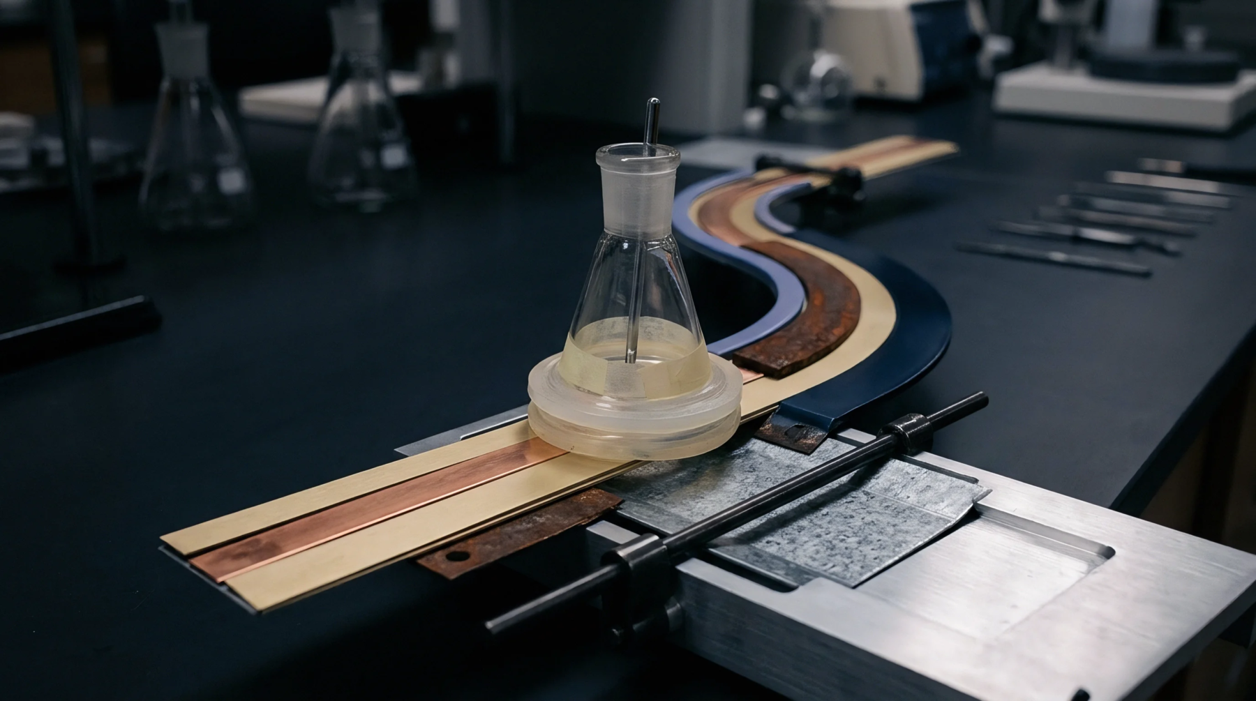
Optimizing boron doping concentrations between 10¹8 and 10¹⁹ cm⁻³ balances high piezoresistive gauge factors with manageable temperature coefficient drift.

Thermal expansion mismatch generates interfacial shear tractions that distort piezoresistive bridge symmetry, producing unrecoverable zero-point drift.
Degenerate boron doping above 5 x 1019 cm-3 bounds radiation mobility loss by saturating impurity scattering in piezoresistive elements.

Moisture ingress causes polymer swelling that transfers mechanical strain to piezoresistive diaphragms, inducing uncompensated zero drift in non-hermetic sensors.

Implantation energy and post-anneal thermal budgets set piezoresistive sensitivity and offset stability in silicon pressure sensor diaphragms.

Dielectric trench isolation on SOI wafers eliminates junction leakage currents, maintaining piezoresistive pressure transducer accuracy above 200°C.

Wafer-level residual stress gradients induce asymmetric die warpage that relaxes over time, causing dynamic calibration matrices to suffer severe cross-axis drift.
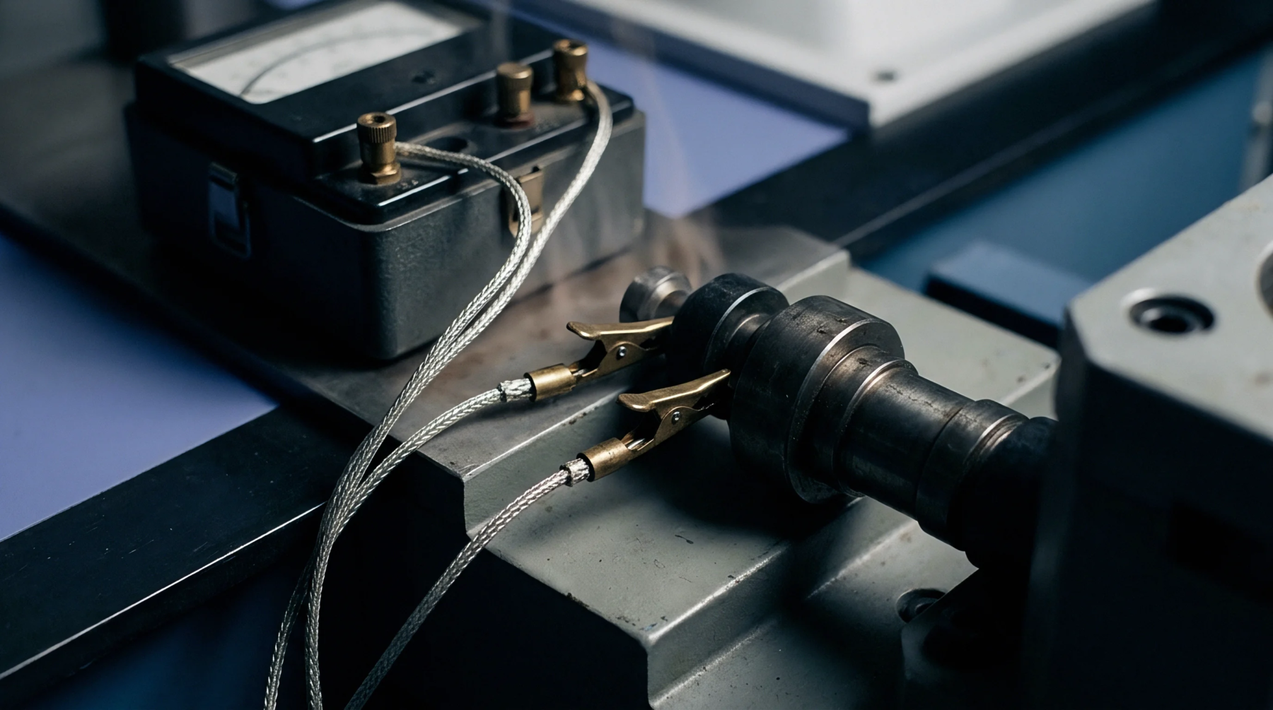
Bivariate polynomial matrix fitting corrects non-linear sensor thermal drift when inputs are normalized and solved via singular value decomposition.

Analytical die stress modeling isolates mechanical package strain from sensor signals while hysteresis compensation algorithms eliminate viscoelastic offset drift.

Analytical shear lag models quantify strain transfer from boards to bottom-terminated packages, showing compliant die attach drops offset drift by 98 percent.

Polymeric underfill modulus collapse near glass transition increases board strain attenuation while driving out-of-plane bump fatigue and sensor drift.

Unbalanced copper planes and high-modulus die attach adhesives in laminate sensor packages cause reflow-induced warpage that shifts piezoresistive zero points.

Compliant silicone buffer layers isolate piezoresistive silicon dies from rigid epoxy cure shrinkage, eliminating offset drift in harsh industrial sensors.
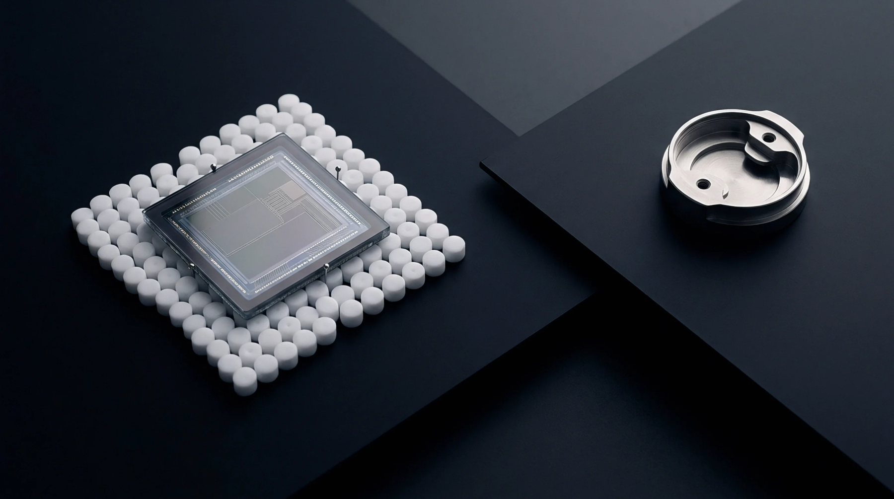
Silicon die thermal expansion mismatches induce structural packaging stresses that warp inertial sensing combs, causing uncorrected thermal bias drift.

Non-linear moisture sorption depresses encapsulant glass transition temperatures, driving premature viscoelastic relaxation that induces persistent transducer zero drift.

Thermally isolates precision references from high-current output stages using symmetrical isometric layout, separate Kelvin return paths, and stress slots.

Engineered boron dopant profiles between 8x10^18 and 2x10^19 cm^-3 balance piezoresistive gauge factor against thermal sensitivity drift in silicon MEMS sensors.

Thermal degradation of silicon piezoresistive coefficients and dopant migration drive irrecoverable sensitivity loss and zero drift above 150 Celsius.

Transient logic heating shifts substrate temperatures, degrading analog front ends without spatial floorplan isolation and matched carrier selection.

Control surface-mount sensor zero offset by isolating board flex with PCB relief slots, selecting low-modulus die attach packages, and balancing solder volume.

Silicone swelling under humidity shifts induces interfacial stress on silicon pressure dies, creating reversible zero drift up to 0.4 percent of full scale.

Viscoelastic package stress relaxation and thermal shock shear fatigue degrade micro-sensor offset stability, requiring void-free compliant die attach.

Lead-free solder creep relaxes reflow shear stress at ambient storage temperatures, tilting MEMS anchors and driving uncalibrated zero drift over time.
Expertise is a utility, not a secret. sentiention™ publishes its working knowledge as open reference: intelligence layer covering the materials it sources, the markets it enters, and the reference that serves both.