Surface Mount Isolation Package Creepage and Clearance Selection Standards
Select surface mount isolation packages by matching CTI material groups and working voltages to mandatory creepage and clearance distances under IEC 60664-1.


Distance
Solid-state isolator safety depends entirely on physical separation between primary and secondary pin banks. When high voltages span across IC terminals, clearance through air and creepage across the package surface dictate whether the part tolerates long-term voltage stress or suffers dielectric breakdown. Common surface-mount packages like standard SOIC-8 provide roughly 4.0 mm of clearance between opposing leads, while wide-body packages push that distance to 8.0 mm, reaching 14.5 mm in stretched variants.
Galvanic Isolation Boundaries in Surface Mount Assemblies
Clearance is the shortest distance through air between input and output pins, shielding the circuit from transient overvoltage arcs. Creepage, by contrast, tracks the shortest route along the outside of the encapsulating resin or board substrate between those terminals. Because dust, moisture, and flux residue degrade dielectric impedance over time, creepage requirements equal or exceed air clearance limits at any given working voltage.
Safety standards divide insulation into basic, supplementary, and reinforced grades. Basic insulation serves as a single protective barrier against shock during normal operation. Reinforced insulation acts as a dual-layer equivalent, calling for twice the clearance and substantially wider creepage so safety remains intact if one barrier fails.
Under IEC 60664-1, an industrial inverter running at 300 Vrms in a Pollution Degree 2 environment requires at least 1.5 mm clearance and 3.0 mm creepage for basic insulation, but shifts to 3.0 mm clearance and 6.0 mm creepage once reinforced ratings apply.
Safety standards under IEC 60664-1 Clause 5.1.2 dictate that reinforced insulation ratings require double the basic insulation creepage metric or a minimum 8.0 mm physical boundary for system working voltages up to 600 Vrms.
Falling short of these spacing thresholds creates distinct failure modes over operating life.
- Creepage Arcing Arc-over develops as surface degradation carves a carbonized conductive path across the molding compound, latching or corrupting the isolator’s logic state.
- Clearance Sparkover Discharge occurs when ionized air allows a high-voltage transient to arc between opposing pin rows, bridging isolated reference grounds.
- Substrate Leakage Drift stems from continuous DC bias driving ionic migration across the PCB surface in humid environments.
- Thermal Cycling Cracking happens when mismatched thermal expansion between the metal leadframe and surrounding epoxy pulls open micro-fissures that ingest contaminants.
Locking in package geometry early avoids redesigning the layout during formal compliance testing.
| Package Type | Body Width (mm) | Lead Pitch (mm) | Min Creepage (mm) | Min Clearance (mm) | Max Working Voltage (Vrms) |
|---|---|---|---|---|---|
| SOIC-8 Standard | 3.90 ± 0.10 | 1.27 ± 0.05 | 4.00 ± 0.15 | 3.90 ± 0.15 | 250 |
| SOIC-16 Wide | 7.50 ± 0.15 | 1.27 ± 0.05 | 8.00 ± 0.20 | 8.00 ± 0.20 | 560 |
| Stretched SO-8 | 6.80 ± 0.10 | 1.27 ± 0.05 | 8.30 ± 0.15 | 8.00 ± 0.15 | 600 |
| DIP-8 Gullwing | 6.35 ± 0.20 | 2.54 ± 0.10 | 7.62 ± 0.25 | 7.00 ± 0.20 | 400 |
| LGA-8 Low Profile | 3.00 ± 0.08 | 0.65 ± 0.03 | 3.20 ± 0.10 | 3.10 ± 0.10 | 150 |

Air Gaps against Solid Surface Tracking Paths
Molded channels along the underside of a component body give package designers a way to lengthen surface paths beyond the straight-line air gap. Cropping internal leadframe pins further opens spatial clearance around active high-voltage nodes. Still, air clearance stays vulnerable to shifts in ambient pressure, while tracking along the package face depends on the mold compound’s resin purity and surface texture.
Standard SOIC footprints cannot clear 1000 VDC solar inverter bus requirements. Stepping up to 14.5 mm stretched SOIC variants meets IEC 62368-1 reinforced insulation tables directly, avoiding hand-formed leads or legacy through-hole optocouplers. Board layouts must preserve that spacing by keeping ground planes and routing away from the isolation zone beneath the package.
Under Annex F of IEC 60664-1, failing an inspection on physical spacing halts safety certification immediately, forcing a layout re-spin before hardware can ship.
Trench
Molded grooves on the underside of specialized packages extend surface creepage without expanding the IC footprint on the board. These recessed channels break up the planar path across the epoxy, forcing any tracking current to navigate down into the relief feature before reaching the opposite pins.
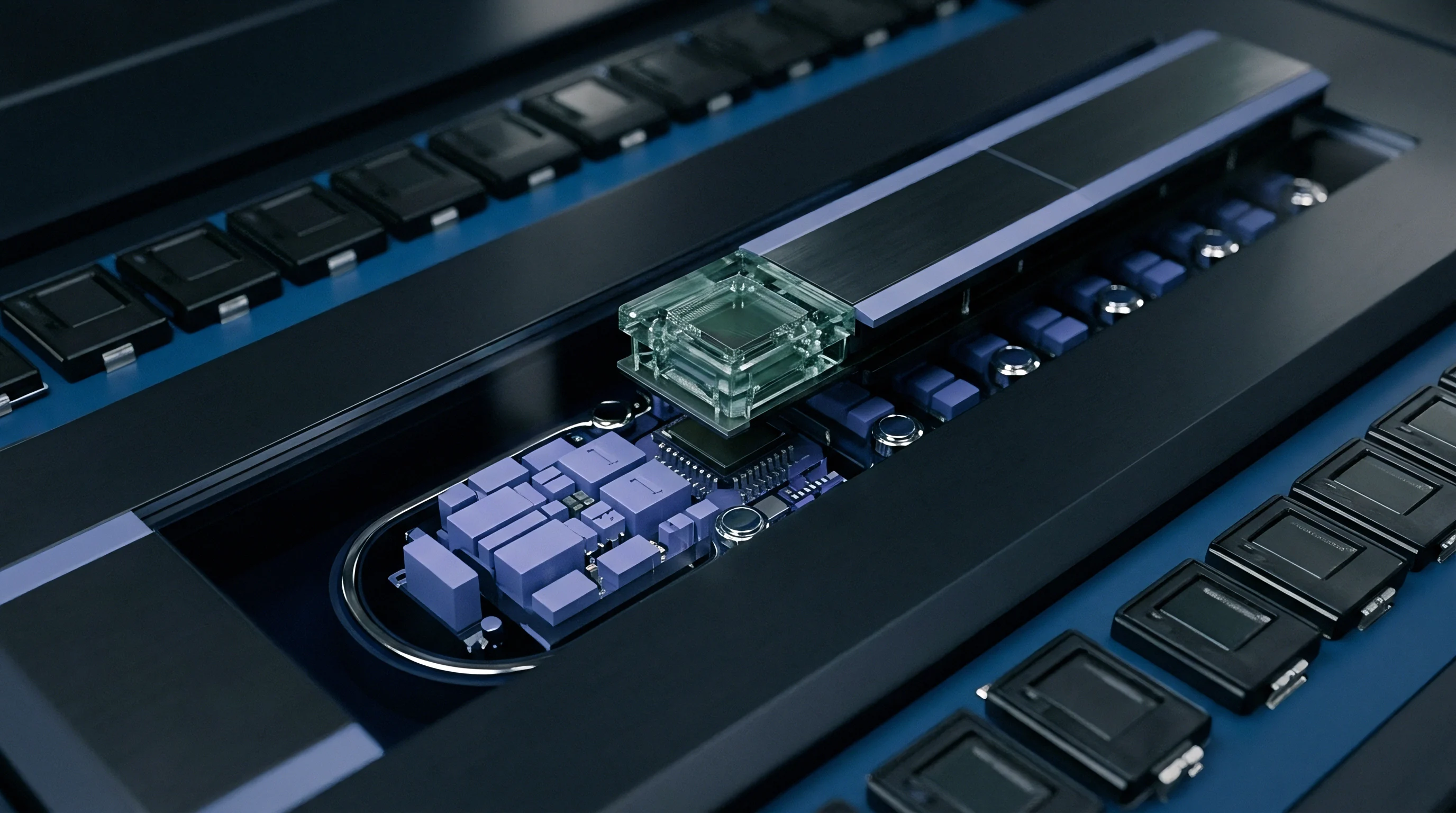
Molded Body Channels and Leadframe Offsets
Underbody slots cut into wide-body SOIC designs satisfy strict 8.0 mm creepage rules inside relatively compact profiles. A molded channel measuring 1.0 mm wide and 1.0 mm deep contributes 2.0 mm of additional tracking distance along the surface without disturbing lead pitch or outer pin-to-pin dimensions.
Creepage paths must incorporate bottom package channels at least 1.0 mm wide to count as true distance additions under industrial pollution specifications.
Internal leadframe geometry must align with outer mold thickness. High-voltage digital isolators place primary and secondary dies on separate copper flags insulated by thin-film silicon dioxide or polyimide layers. If the outer molding compound lacks surface resistance in humid air, high-voltage stress breaches the external package long before the internal barrier breaks down.

Comparative Tracking Index Classifications for Epoxy Compounds
Component molding compounds are categorized by Comparative Tracking Index ratings established through IEC 60112 liquid drop tests. The test deposits droplets of ammonium chloride electrolyte onto the plastic specimen under an AC bias until a conductive tracking path forms.
| Material Group | CTI Rating Range (V) | Tracking Resistance Level | Altitude Range (m) | Clearance Multiplier |
|---|---|---|---|---|
| Group I | CTI ≥ 600 | Exceptional | Up to 2000 | 1.00 |
| Group II | 400 ≤ CTI < 600 | High | 2001 to 3000 | 1.14 |
| Group IIIa | 175 ≤ CTI < 400 | Moderate | 3001 to 4000 | 1.29 |
| Group IIIb | 100 ≤ CTI < 175 | Basic | 4001 to 5000 | 1.48 |
Specifying a Material Group IIIa package instead of Group I forces the PCB layout to widen surface distances by up to 40 percent for the exact same working voltage. Because commercial datasheets frequently omit explicit CTI ratings, engineering teams generally have to pull factory qualification reports to verify the resin grade.
In humid operating environments, packages with lower CTI ratings eventually suffer localized tracking, dendritic carbon growth across the underside, and permanent barrier failure.

Slot
Milling an air slot through the PCB substrate underneath a surface-mount isolator raises surface insulation margins on crowded boards. Routing away the FR-4 laminate between primary and secondary pads converts a creepage path into an air clearance gap, removing substrate tracking risks when heavy condensation forms.

How Does PCB Slot Width Affect Isolation Margin?
Under IEC 60664-1, a routed slot 1.0 mm wide or greater turns what would be a creepage calculation along the laminate into a clearance measurement through air. Where an un-slotted SOIC-16 wide body on FR-4 delivers 8.0 mm creepage under Pollution Degree 2, dropping a 1.2 mm cutout beneath the chip creates an air gap adequate for Pollution Degree 3 conditions.
Dust and ambient moisture settle into cutouts if enclosure airflow is stagnant, introducing ionic contamination over time. Because solder flux leaves a conductive residue, assembly processes using no-clean chemistry need to track ionic contamination and stay below 1.56 µg/cm² NaCl equivalent to avoid leakage bridging the slot.
A PCB routing slot narrower than 1.0 mm fails to break surface tracking paths under IEC safety guidelines, offering zero creepage distance improvement over intact board surfaces.
High-voltage board layouts require disciplined boundary routing to keep dielectric flashovers from developing.
- Keep-out Zone Enforcement requires clearing all copper traces, ground planes, and signal vias within an 8.0 mm boundary around isolation pads.
- Solder Mask Dam Control maintains at least a 0.1 mm solder mask dam between adjacent isolator pads to prevent bridging during reflow.
- Slot Edge Separation keeps at least 0.5 mm of laminate between copper pad borders and the routed edge so copper does not lift during routing or assembly.
- Edge Chamfering Precision clears away burrs and protruding glass fibers along the routed slot edge to maintain an unobstructed air clearance channel.

Solder Mask Integrity and Surface Contamination Traps
Liquid photo-imageable solder mask offers basic surface insulation, but standards do not credit it as a solid dielectric barrier. Thermal shock during reflow often opens micro-cracks around IC leads that trap flux salts and moisture, setting up low-impedance leakage paths across high-voltage terminals.
Routing traces beneath surface-mount isolators undermines isolation ratings. Any conductor passing under the IC body reduces effective clearance to the distance between the pin and the copper beneath it, invalidating isolation calculations.
Edge-milled board cutouts increase router bit wear and fabrication cycle times, often prompting PCB shops to propose un-plated silkscreen markings as alternatives that provide none of the physical clearance of a true slot.

Impulse
Isolators deployed in solar inverters, EV chargers, and motor drives endure frequent voltage transients from lightning strikes and inductive load switching. Testing under UL 1577 and IEC 60747-17 screens these isolation barriers against short-duration, high-voltage impulses to ensure physical dielectric integrity.

Transient Surge Stresses and Dielectric Withstand Limits
Isolators must handle continuous peak working voltages alongside transient overvoltages up to 12.8 kV without breakdown or internal delamination. Optocouplers certified to UL 1577 undergo 100 percent production testing with a 1-second AC proof test at 120 percent of rated isolation voltage, typically rated at 3.75 kVrms or 5.0 kVrms.
Capacitive and magnetic isolators fall under IEC 60747-17, requiring surge testing up to 10 kV peak. Transient voltages stress the bond line between the internal die encapsulation and the external package mold compound. Microscopic voids along the leadframe trigger partial discharge under strong electric fields, slowly eating away at the internal dielectric over years in service.
Qualification relies on a defined test sequence to confirm isolation ratings under stress.
- Precondition test samples by baking at 125 °C for 24 hours to expel trapped moisture from the package bodies.
- Condition units for 168 hours at 85 °C and 85 percent relative humidity in accordance with JEDEC J-STD-020.
- Run parts through three successive lead-free reflow profiles peaking at 260 °C to simulate board assembly stress.
- Tie primary and secondary pin groups into two separate shorted nodes using high-voltage test fixtures.
- Inject a 1.2/50 µs surge waveform across the two terminal sets, stepping up in 500 V increments to the peak test limit.
- Measure partial discharge at 1.5 kVrms, verifying that discharge activity stays below 5 picocoulombs.

Altitude Amplification and Working Voltage Calculations
Air density drops with elevation, reducing the breakdown strength of air gaps across external pins. Because of this, IEC 60664-1 specifies clearance multiplication factors whenever equipment operates above 2000 meters.
A solar inverter operating at 4000 meters elevation requires clearance values scaled by 1.29. A package calling for 8.0 mm clearance at sea level needs 10.32 mm of air separation at 4000 meters. This correction factor applies only to air clearance; required creepage across solid package surfaces remains the same regardless of altitude.
As wide-bandgap designs push switching transitions past 100 V/ns, whether high dv/dt accelerates surface tracking across sub-millimeter leadframes remains a central concern for power system architects.

Tariff
Part selection balances isolation headroom against component cost, reel packaging fees, and occupied PCB space. Standard SOIC-8 devices carry a substantial cost advantage over stretched wide-body alternatives, though limited baseline creepage restricts them to lower working voltages.
Bill of Materials Impact of Stretched SOIC Packages
Moving from a standard 4.9 mm x 3.9 mm SOIC-8 package to an 11.5 mm x 7.5 mm stretched SOIC-8 expands the component land pattern by more than 300 percent. The extra epoxy mold volume and broader leadframe also drive a unit price premium across every production tier.
| Package Variant | PCB Area (mm²) | Isolation Rating (kVrms) | Unit Cost @ 1k ($) | Unit Cost @ 50k ($) | Tape & Reel Standard |
|---|---|---|---|---|---|
| SOIC-8 Standard | 31.0 | 2.5 | 0.42 ± 0.03 | 0.24 ± 0.02 | 2,500 pcs/reel |
| SOIC-16 Wide | 108.0 | 5.0 | 1.15 ± 0.08 | 0.68 ± 0.04 | 1,000 pcs/reel |
| Stretched SO-8 (8.3mm) | 86.2 | 5.0 | 0.95 ± 0.06 | 0.54 ± 0.03 | 1,500 pcs/reel |
| LGA-8 Dual-Pad | 15.0 | 1.5 | 0.65 ± 0.04 | 0.38 ± 0.02 | 3,000 pcs/reel |
Wide-body packages require larger pick-and-place nozzles and wider feeder spacing on high-speed SMT lines. In dense assemblies, using ultra-compact LGA isolators alongside milled slots preserves creepage while keeping board area to a minimum.

Yield Rates and Placement Densities across Package Options
Fine-pitch LGA isolators suffer higher rates of solder bridging during reflow than wide-body leaded SOIC packages. A 0.65 mm pitch pad array demands tight aperture tolerances, typically requiring 100-micron electro-polished stainless steel stencils for clean paste release.
Comparing an integrated wide-body digital isolator against a discrete optocoupler circuit favors the integrated route on total area. Discrete optocouplers require bias resistors, drive transistors, and decoupling capacitors that double part counts and consume extra routing space.
Designing with standard package forms across high-volume product lines secures supply chain flexibility, while custom high-creepage packages create single-source risks during global component shortages.
Defaulting to wide-body packages with 8.0 mm creepage in high-voltage SMT designs prevents costly board redesigns and safety re-testing if the product family later moves into higher-voltage industrial applications.