Precision Voltage Reference Layout Mechanics for Circuit Designers
Precision voltage reference layout demands mechanical isolation slits, symmetric thermal copper paths, and compliant leads to eliminate piezoresistive drift.

Strain
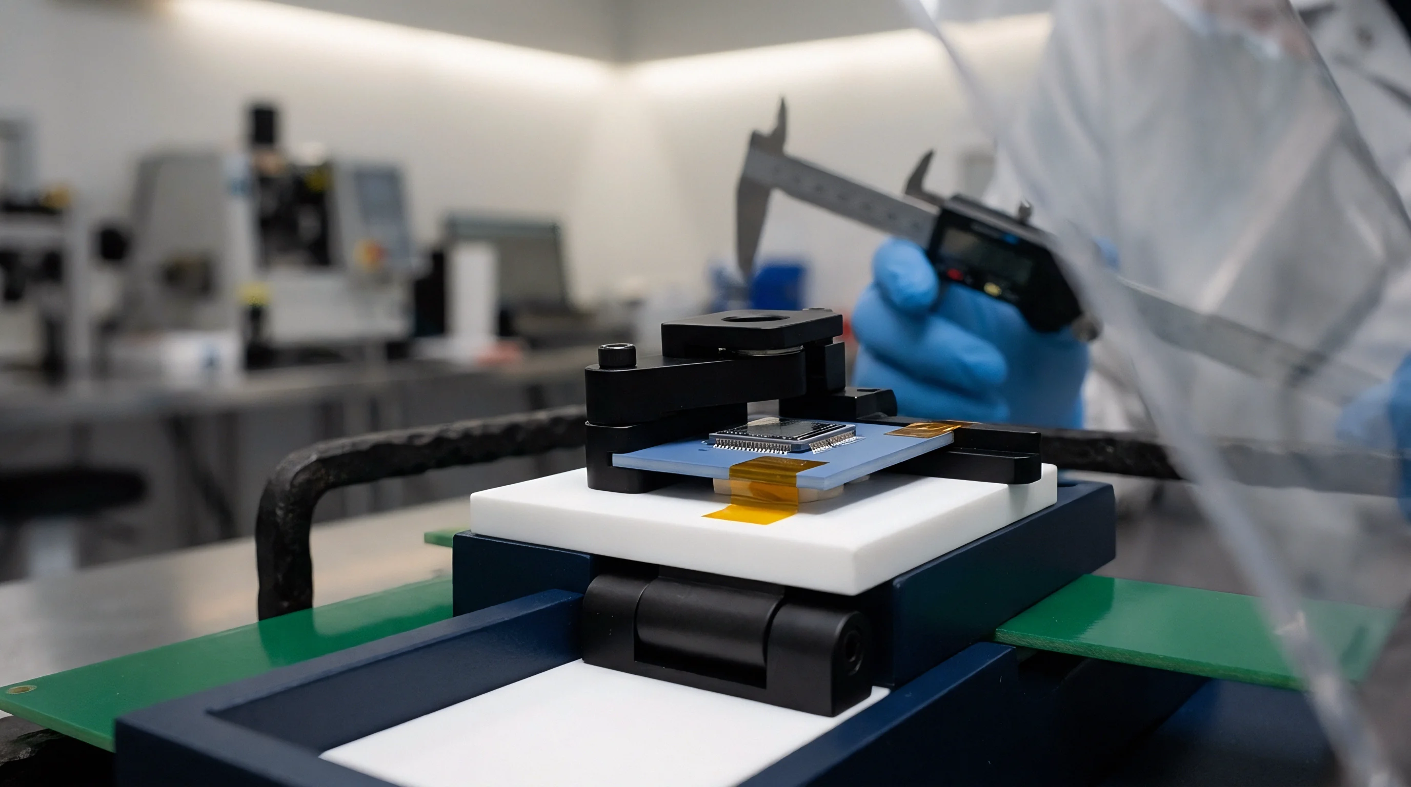
Precision bandgap and buried Zener references shift output voltage whenever external forces deform the encapsulated silicon die. Silicon has marked piezoresistive sensitivity, turning localized mechanical shear and normal stress into changes in carrier mobility, junction potentials, and thin-film resistor values. When a surface-mount reference is soldered onto an FR-4 board, differential thermal expansion between the copper-clad laminate and the package material locks residual stress into the leadframe or substrate.
That trapped stress pulls the reference potential away from its factory trim value.
Plastic packages like SOIC-8, MSOP-8, and SOT-23 undergo heavy baseline shifts during reflow. Below their glass transition temperature, standard epoxy mold compounds expand at 12 to 18 parts per million per degree Celsius, compared to roughly 16.5 parts per million for copper leadframes and 2.6 parts per million for silicon. As solder solidifies at SAC305’s 217-degree Celsius liquidus point and cools to room temperature, this uneven contraction clamps the internal die under compressive stress exceeding 80 megapascals.
On a 2.500-volt buried Zener core, the resulting 100 to 500 microvolt shift can consume the entire factory tolerance before the circuit ever operates in the field.
FR-4 substrates cooled from lead-free reflow peak temperatures transmit compressive die stresses exceeding fifty megapascals through molded plastic leadframes.
Ceramic leadless chip carrier packages avoid moisture swelling, but they anchor rigidly to the board surface. LCC packages lack compliant leads, so solder joints carry board flex directly into the ceramic base. Multi-layer ceramic deforms very little from thermal effects alone, but physical board bending passes shear strain straight across the castellations.
Package Form Distortion Mechanics
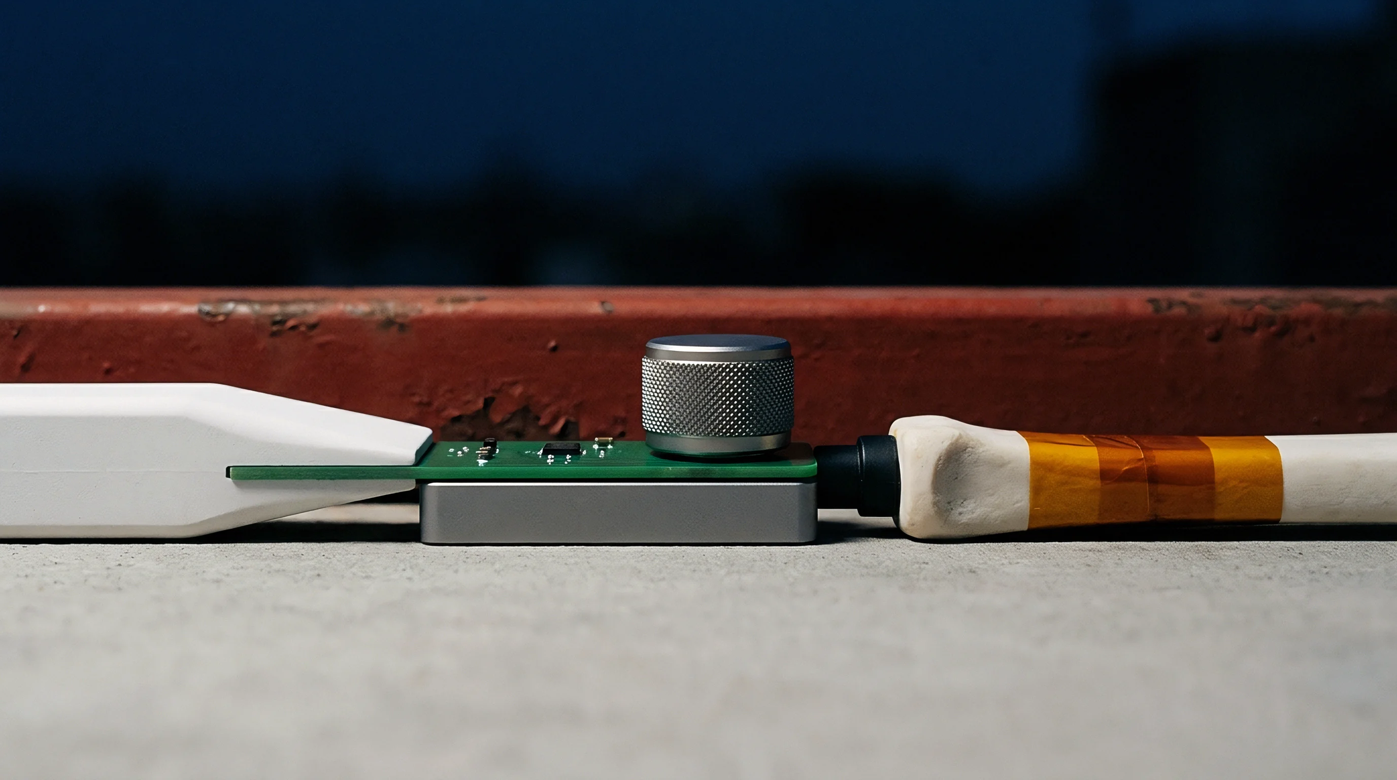
Mechanical stress travels from the mounting pads to the die attach paddle along distinct physical paths. Gull-wing leads on narrow-body SOIC packages offer compliance along the lateral axis, dampening board flex compared to bottom-pad terminations. By contrast, Quad Flat No-Lead packages solder an exposed thermal pad straight to internal ground planes, removing compliance and coupling stress directly into the die.
Achieving sub-ppm long-term drift requires isolating the reference from board strain through careful package selection and physical decoupling.
| Package Configuration | Lead Compliance Axis | Substrate Thermal Expansion | Typical Reflow Output Shift | Moisture Swell Susceptibility |
|---|---|---|---|---|
| SOIC-8 Gull-Wing | Bi-directional lateral | 15.5 ppm per degree C | 75 to 250 ppm | Moderate (0.3 percent mass uptake) |
| Ceramic LCC-8 | Non-compliant castellation | 6.5 ppm per degree C | 15 to 40 ppm | Zero (hermetic cavity) |
| VSSOP-8 Gull-Wing | Short-radius lateral | 14.0 ppm per degree C | 120 to 350 ppm | High (thin package wall) |
| TO-46 Metal Can | Omni-directional through-hole | 5.2 ppm per degree C | 5 to 15 ppm | Zero (welded metal seal) |
| DFN-8 Exposed Pad | Zero compliance anchor | 16.0 ppm per degree C | 200 to 600 ppm | High (exposed bottom copper) |
Rigid metal cans preserve factory calibration through physical separation. Packages like the TO-46 or TO-99 suspend the active die platform above the board surface on gold-plated Kovar leads, absorbing board movements through lead flexure. Paying forty dollars for a hermetic metal package buys mechanical strain isolation rather than fundamentally superior silicon.
Surface-mount plastic packages require careful layout countermeasures to approach that same isolation.
Torsional strain occurs whenever mounting hardware fastens a board into an uneven chassis. Applying three Newton-meters to a corner screw creates diagonal warpage through nearby traces and internal copper planes. Precision references seated near these mounting holes register microvolt-level baseline shifts as the fasteners are tightened, permanently skewing the measurement chain.


Slit
Milled routing grooves cut into the laminate block the propagation of mechanical shear stress. Securing a board into an enclosure flexes the substrate along its mounting axes, and solid FR-4 carries that flex across thousands of mils to distort every footprint in its path. Cutting an isolation slit between the mounting points and the reference interrupts strain transfer by creating a compliant sub-island.
Effective strain relief relies on U-shaped or rectangular drop-out slots around three sides of the footprint, creating a cantilevered tongue with the reference sitting on the free end. Because mechanical isolation improves as the connecting neck narrows, layout design becomes a compromise between physical robustness and strain stability. On a standard 1.6-millimeter FR-4 board, a 2.5-millimeter neck reduces strain transmission by over twenty decibels relative to a solid plane.
Slot Geometry and Keep-Out Bounds
Milling tolerances dictate minimum clearances near surface-mount landing pads. Standard mechanical routing bits run 0.8 to 1.6 millimeters in diameter, setting minimum slot widths on dense layouts. Copper features ending near a milled edge need at least 0.5 millimeters of clearance to avoid burrs, copper tearing, and conductor exposure during edge profiling.
Cutting tighter than this lets router bit vibration crack internal via barrels beneath component pads.
- Routing keep-out evaluation verifies that no inner layer power or signal traces cross the perimeter of the milled slots, preventing severed connections during board fabrication.
- Bridge width proportioning sets the mechanical anchor dimension between 2.0 and 3.0 millimeters, retaining sufficient rigidity for automatic pick-and-place nozzle pressure.
- Decoupling capacitor localization places supply bypass components directly on the isolated island, eliminating trace inductance across the mechanical isolation neck.
- Singulation edge setback distances the voltage reference at least twenty millimeters away from scored v-grooves or punch-de-paneling boundaries to prevent transient shock damage.
High-vibration environments restrict the use of thin cantilevered tongues. Under cyclic acceleration, an isolated board tongue acts like a spring-mass system with a specific resonant frequency. If vehicle motion or cooling fan turbulence matches this resonance, the tongue oscillates violently and drives alternating cyclic stress into the solder joints, accelerating fatigue.
Industrial designs for mobile equipment drop cantilever tongues in favor of four-slot perimeter patterns held by two opposing bridges.
Thermal Symmetry across Slots
Mechanical slots double as high-resistance thermal barriers. FR-4 conducts heat in-plane at roughly 0.8 watts per meter-Kelvin, while air inside a slot conducts only 0.026 watts per meter-Kelvin. Heat from nearby power regulators, microcontrollers, or power transistors cannot cross the air gap, keeping dynamic board thermal waves off the reference island.
As a result, the die tracks ambient temperature instead of board power dissipation.
Islands must balance heat loss evenly to keep internal gradients from forming. Asymmetrical copper distributions across an isolated peninsula set up directional heat paths. When air movement cools one edge faster than the other, thermoelectric offsets develop across device terminals.
Keeping copper planes symmetric across the bridge preserves a uniform temperature across the landing zone.
Placing sensitive silicon platforms on cantilevered board tongues eliminates board-level strain while demanding strict balance against environmental vibration.
Routing traces across the supporting neck takes strict discipline. Only essential analog signal, reference output, and local ground traces should make the crossing. Nearby digital bus lines cause capacitive crosstalk and stiffen the narrow laminate corridor mechanically.
Keeping line counts down preserves physical compliance while keeping the bridge cross-section as small as possible.

Copper
Connecting reference pins to circuit traces creates inadvertent thermocouples. The Seebeck coefficient between copper traces and Alloy 42 leads runs up to thirty-five microvolts per degree Celsius, while copper-to-Kovar contacts generate about forty microvolts per degree Celsius. Ordinary SAC305 lead-free solder generates two to three microvolts per degree Celsius against pure copper.
A thermal gradient of just 0.1 degrees Celsius between the positive output pin and ground reference pin introduces an unrecoverable DC error into a six-digit measurement path.
Thermal symmetry governs all trace layouts coming off the component footprint. Traces attached to differential terminals need identical copper widths, weights, and routing paths. Dumping one pin into a massive ground flood while taking the adjacent pin out through a thin eight-mil trace creates an immediate offset, as heat pulls away quickly from ground while staying trapped in the output line.

Symmetric Footprint Realization
Equalizing thermal mass requires matched copper fills on every functional lead. When a ground pin ties into an internal plane, it should use thermal relief spokes identical to the necked output trace. Flooding solid copper over one side of an SOIC footprint while leaving opposing pins on narrow signal traces warps the thermal field across the die paddle.
- Thermal relief cross-spokes restrict direct heat conduction into wide ground planes, matching the thermal resistance of adjacent signal conductors within five percent.
- Dummy thermal pads balance heat sinking on non-connected pins, preventing unilateral heat extraction from one side of the silicon substrate.
- Parallel routing paths keep output lines and return lines in close physical proximity, exposing both conductors to identical external thermal drafts.
- Enclosure isolation walls shield the reference copper footprint from localized airflow induced by internal cooling fans or convection chimneys.
Kelvin connections prevent trace resistance errors under changing load currents. An eight-mil trace on one-ounce copper presents about 0.017 ohms of DC resistance per hundred millimeters. If a downstream ADC or op-amp stage draws five milliamperes of dynamic current through that line, the drop is eighty-five microvolts.
Force-sense routing brings the measurement feedback loop directly to the pin pad, removing track resistance from the signal path.
| Interconnect Material Interface | Seebeck Coefficient | Error per 0.5 Deg C Gradient | Error Relative to 2.5V 16-Bit LSB |
|---|---|---|---|
| Copper to Alloy 42 (Standard SOIC Leads) | +35.0 microvolts per deg C | 17.5 microvolts | 0.46 LSB |
| Copper to Kovar (TO-46 and LCC Contacts) | +40.0 microvolts per deg C | 20.0 microvolts | 0.52 LSB |
| Copper to SAC305 Solder (Lead-Free Joint) | +2.5 microvolts per deg C | 1.25 microvolts | 0.03 LSB |
| Copper to SnPb 63/37 (Leaded Solder Joint) | +1.8 microvolts per deg C | 0.90 microvolts | 0.02 LSB |
| Copper to Copper-Oxide Interface (Corroded Pad) | +1000 microvolts per deg C | 500 microvolts | 13.10 LSB |
Ground loops introduce unwanted common-mode shifts through resistive coupling. Precision references rely on a clean star-ground return back to the system ADC ground plane. Sharing return paths with clock buffers, microprocessors, or PWM switching regulators dumps high-frequency noise and ground bounce straight into the reference core.
Layouts must keep analog reference returns separated from noisy grounds right up to their single star point.
Trace routing falls entirely within customer domain responsibility when parts fail to meet datasheet accuracy.
Drift
Datasheet drift specifications cover behavior under clean, unstressed test conditions, where socketed parts rest in temperature-controlled baths with no board stress present. Once an automated pick-and-place machine drops the part onto FR-4 and sends it through a 260-degree reflow oven, long-term stability degrades through stress relaxation, epoxy hydration, and chemical migration.
Hygroscopic expansion in plastic packages is a primary cause of uncalibrated reference drift. Epoxy molding compounds absorb moisture from surrounding air until reaching equilibrium with ambient humidity. This water uptake expands the epoxy volume by 0.1 to 0.4 percent, loading fresh compressive and tensile stresses onto the die surface.
A reference trimmed cleanly in a dry lab will drift twenty to sixty parts per million when operated in an environment at eighty percent relative humidity.
Moisture Swell Mitigation and Baking Schedules
Baking assembled boards drives trapped moisture back out of mold compounds, restoring output levels toward post-reflow dry values. Re-absorption starts as soon as assemblies return to unconditioned air, however. Conformal coatings like polyurethane, silicone, or acrylic slow moisture entry but cannot stop it long-term.
Real moisture immunity requires hermetic packages or complete potting structures.
- Dehydration pre-bake holds the bare printed circuit boards at 125 degrees Celsius for four hours prior to component population, eliminating internal laminate water pockets.
- Reflow peak limitation keeps peak component temperature below 245 degrees Celsius to reduce thermal shock degradation of internal passivation layers.
- Post-assembly burn-in powers the completed board assemblies at 85 degrees Celsius for 168 hours to accelerate the release of initial thermo-mechanical assembly strain.
- Secondary stabilization rest stores unpowered assemblies at ambient laboratory conditions for seventy-two hours, permitting dielectric polarization to reach equilibrium.
Piezoresistive settling continues for hundreds of hours after soldering. Leadframes and FR-4 slowly ease residual reflow tension through microscopic mechanical slippage at epoxy-glass interfaces. This relaxation shows up as drift that decays logarithmically over time.
Calibrating immediately after assembly bakes these temporary offsets into memory, degrading absolute system accuracy as the board settles during its first month in service.
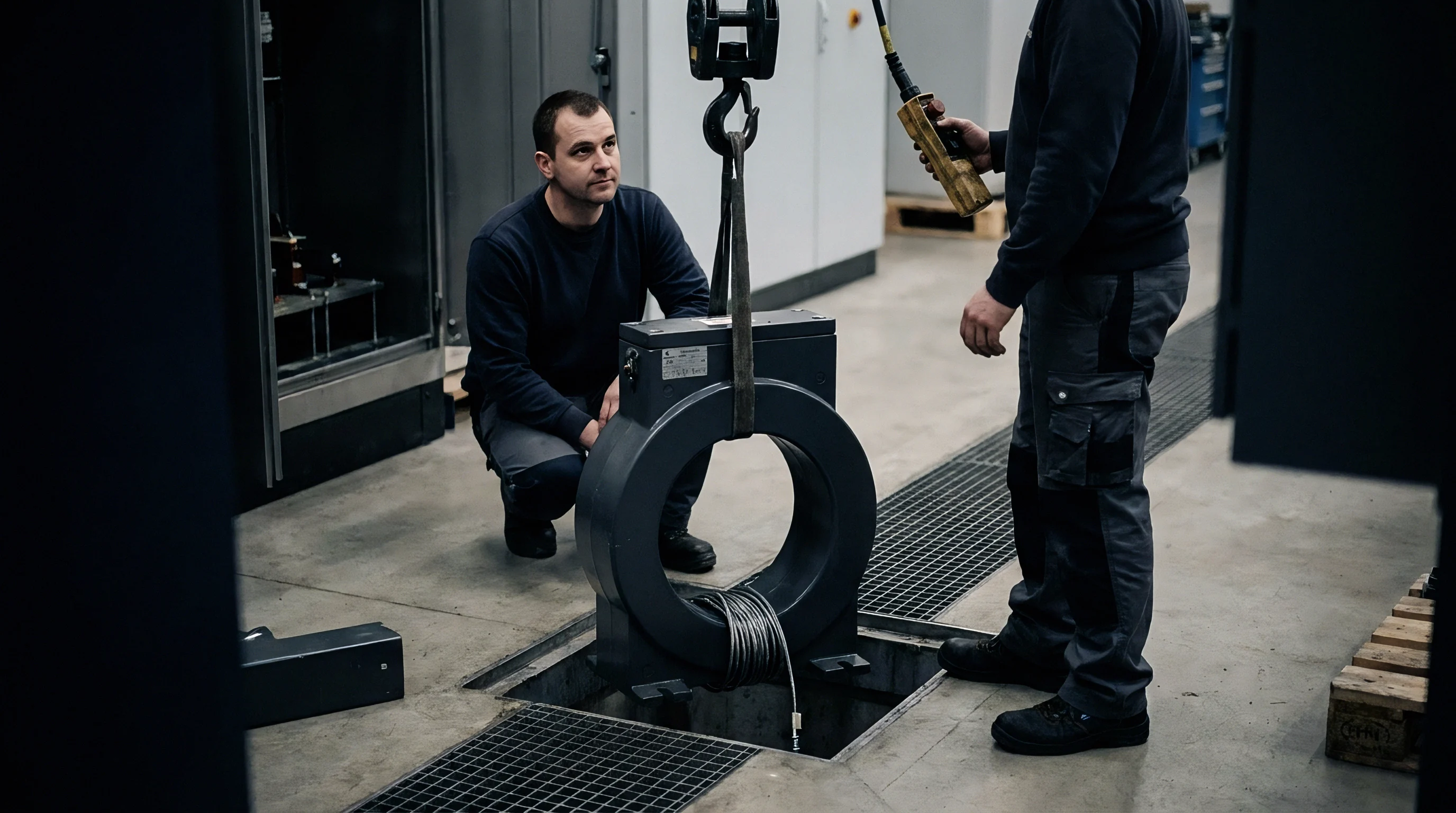
Thermal Hysteresis Boundaries
Thermal hysteresis reflects a reference’s inability to return to its original output voltage following a temperature excursion. When equipment cycles from room temperature down to minus forty degrees Celsius and back, internal materials trace different stress-strain paths during cooling and heating. Mold compounds exhibit mechanical hysteresis, leaving permanent changes in residual die stress after thermal cycles.
IPC J-STD-033 specifies handling constraints that dictate dry packaging requirements for plastic surface-mount devices sensitive to atmospheric hydration.
Buried Zener references handle thermal hysteresis much better than standard bandgap designs. A typical bandgap reference in an SOIC shifts thirty to seventy parts per million across a minus forty to plus eighty-five degree Celsius cycle. A buried Zener in a ceramic LCC shifts under five parts per million over that same range, demonstrating how much mechanical package choices influence repeatable performance.


Solder
Solder alloy selection defines the baseline compliance of every surface-mount joint. Standard 63/37 tin-lead solder has an elastic modulus of around thirty-two gigapascals, yielding under plastic shear deformation to absorb modest board flexure. Lead-free SAC305 has a modulus of fifty-one gigapascals, making a far stiffer connection that transmits fifty-nine percent more board flex into the package.
On standard FR-4 assemblies, that extra stiffness can triple post-assembly output shifts.
Stencil aperture design sets solder volume and standoff height under terminals. Low standoffs squish the solder into a thin layer that cannot yield under mechanical or thermal loads. Increasing the distance between PCB copper and the package lead adds joint compliance, taking up lateral expansion differences.
Stencil cuts made 1:1 to landing pads often apply too much paste, building heavy fillets that climb gull-wing leads and eliminate their engineered flex.
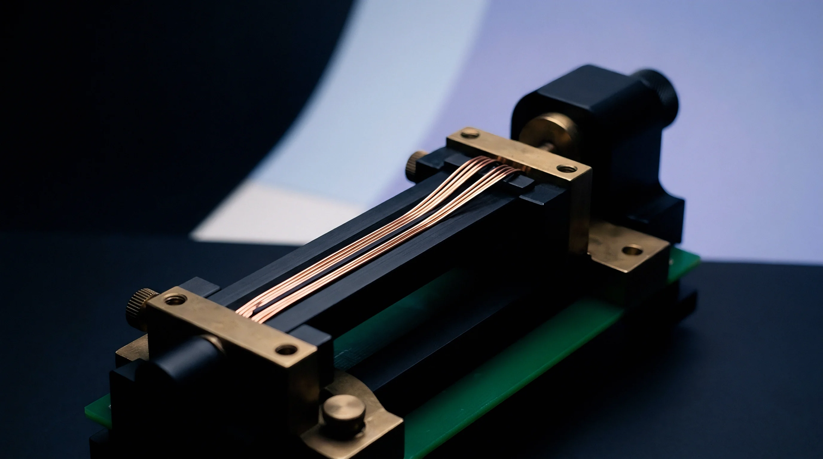
Aperture Reduction and Fillet Control
Reducing stencil aperture area to eighty-five percent of the land footprint prevents solder balling and controls wetting up the lead heel. A moderate fillet securing the toe while leaving the upper radius free preserves the spring rate of gull-wing pins. On bottom-terminated Quad Flat No-Lead packages, over-soldering the large center pad tilts the component body, creating concentrated local die stress.
| Alloy Composition | Liquidus Temperature | Elastic Modulus | Yield Strength | Shear Strain Transmission |
|---|---|---|---|---|
| Sn63Pb37 (Eutectic Leaded) | 183 degrees C | 32.1 gigapascals | 39.5 megapascals | Baseline reference |
| Sn96.5Ag3.0Cu0.5 (SAC305) | 217 degrees C | 51.0 gigapascals | 43.0 megapascals | 59 percent above SnPb |
| Sn42Bi58 (Eutectic Low-Temp) | 138 degrees C | 40.0 gigapascals | 55.0 megapascals | 25 percent above SnPb |
| In97Ag3 (Indium High-Compliance) | 143 degrees C | 10.5 gigapascals | 5.8 megapascals | 67 percent below SnPb |
| Sn99.3Cu0.7 (Low-Cost Lead-Free) | 227 degrees C | 46.0 gigapascals | 35.0 megapascals | 43 percent above SnPb |
High-reliability aerospace and defense hardware sometimes uses indium-bearing solders for sensitive analog blocks. Indium-silver alloy with three percent silver yields an elastic modulus below eleven gigapascals, creating a soft joint that absorbs strain effectively. Indium comes with clear trade-offs, though, including high material cost, limited availability, and potential corrosion risks in humid operational conditions.
Underfill creates a continuous epoxy bridge between component bodies and substrates. While useful for spreading mechanical stress in BGAs to pass drop testing, underfilling a precision reference creates a severe mechanical bridge. Standard capillary underfill shrinks one to two percent as it cures, pulling inward with enough force to shift factory bandgap trims permanently.
Conformal coatings require similar care; low-modulus silicone formulations avoid the lateral clamping caused by rigid epoxy coats.
Unresolved questions persist regarding whether low-temperature bismuth-tin solders can guarantee twenty-year metallurgical stability without micro-cracking when subjected to ongoing mechanical vibration on compliant board tongues.