Addressing Multi Channel Sensors on Shared Two Wire Serial Buses
Addressing multi-channel sensors on shared two-wire buses relies on address pin strapping, active bus switches, or in-line offset address translation ICs.
Node
Silicon vendors restrict the address pins on multi-channel sensors to keep package sizes down and conserve pin count. Most sensor ICs on two-wire serial buses rely on standard seven-bit addressing, which allows for 128 theoretical locations. Because standard allocations reserve sixteen of those for bus management functions, 112 remain available for peripheral devices.
When board layouts require sixteen or thirty-two identical environmental or motion sensors, that hardware address space fills up almost immediately.
Running multiple identical sensing ICs on a single clock and data pair quickly exposes physical layout constraints. Packaging styles like quad flat no-lead (QFN) or wafer-level chip-scale packages (WLCSP) routinely break out only one or two address select lines, typically marked A0 and A1. Pulling those pins to logic high, grounding them, or leaving them floating yields four distinct hardware addresses at most.
Placing a fifth identical sensor on the same bus without some form of isolation creates an immediate address conflict.
Pin Strapping Hardware Constraints
Address selection typically depends on external resistor pull-ups and pull-downs referenced to supply rails or ground. Some sensor packages provide extra flexibility by allowing direct connections to the serial clock or data lines, or by using an internal ADC to decode external resistor divider ratios during power-on reset. Internal logic samples the voltage levels on these pins during the chip’s initial power-up sequence.
Resistor-ratio decoding conserves pin real estate while providing eight or sixteen address options. These networks require precision metal film resistors with one percent tolerance; a drift greater than two percent will cause the internal comparator to select the wrong offset during power-on bias routines. Thermal expansion, flux residue, and board flexing all induce resistance shifts that can lead to incorrect addressing on cold boots.
Fast-mode bus operations at 400 kHz fail when total trace capacitance exceeds 400 pF across interconnected slave devices.
Address Collisions in Multi Sensor Topologies
When duplicate slave addresses share a two-wire bus, multiple devices respond simultaneously during acknowledgment cycles. If a master issues a start condition followed by an address byte shared by two peripherals, both pull the open-drain data line low during the ACK phase, driving the bus concurrently and corrupting the transfer.
Data corruption escalates during read operations as multiple devices attempt to stream internal registers at the same time. Any target driving a logic low overrides another driving a high, forcing dominant zeros into the payload. The host microcontroller then receives invalid bitstreams with broken CRC checksums or nonsensical readings.
Left unhandled, these collisions push firmware drivers into endless retry loops that waste processor cycles and raise current draw.
| Package Type | Pin Count | Address Pins | Decoding Logic | Max Unique Addresses |
|---|---|---|---|---|
| DFN-10 | 10 | 2 (A0, A1) | 3-State Logic Level | 4 |
| QFN-16 | 16 | 3 (A0, A1, A2) | Binary Logic Level | 8 |
| WLCSP-12 | 12 | 1 (ADDR) | 4-Level Resistor Divider | 4 |
| SOIC-8 | 8 | 2 (A0, A1) | Binary Logic Level | 4 |
Failing to verify address budgets during schematic design routinely stalls board bring-up, leading to unpopulated test boards and scrapped assembly runs.

Switch
Active channel multiplexers isolate bus segments by routing clock and data lines through internal field-effect transistors. These bidirectional solid-state switches function as addressable gates, enabling a host controller to select downstream channels via serial control registers. By placing identical sensor addresses on isolated branches, dense layouts can scale without addressing conflicts.
Devices like the TCA9548A provide eight bidirectional pass channels between upstream and downstream lines. The host controller writes to the multiplexer’s fixed address, setting a control byte to enable one or more downstream branches. Keeping inactive channels isolated prevents collisions between sensors that share identical hardware addresses on separate branches of the switch matrix.

Multiplexer Channel Isolation Mechanics
Bidirectional pass gates divide total bus capacitance into discrete downstream branches that stay electrically disconnected until enabled by register writes. Traces on disabled lines do not load the primary bus segment driven by the master, preserving signal integrity across complex board layouts populated with dozens of sensor ICs.
Engaging a channel introduces internal pass-gate resistance, typically 4 ohms to 20 ohms depending on supply voltage. Downstream pull-up resistors keep disabled lines tied to local rails so they maintain valid logic high levels while the primary bus operates. When the host enables a channel, internal FETs conduct, joining upstream and downstream lines without modifying the underlying bit framing.
Standardized Bus Isolation Procedure
Dedicated hardware reset lines provide a recovery path against bus lockups before downstream reconfigurations begin.
- Apply a low-level pulse to the hardware reset pin of the bus multiplexer for a minimum duration of 500 ns.
- Write control byte 0x01 to the multiplexer address to select channel zero while isolating all remaining downstream buses.
- Execute an I2C read transaction to confirm acknowledgment from the sensor populated on the active downstream channel.
- Iterate channel selection register writes from 0x02 to 0x80 to query subsequent isolated downstream buses sequentially.
- Issue register write 0x00 to deselect all downstream channels before putting the main bus into an idle state.
Intermittent downstream faults can hold multiplexer pass gates in a conducting state and prevent channel switching. Corrupt transactions on shared channels often stem from internal switch channel leakage rather than transient ground bounce.

Translation
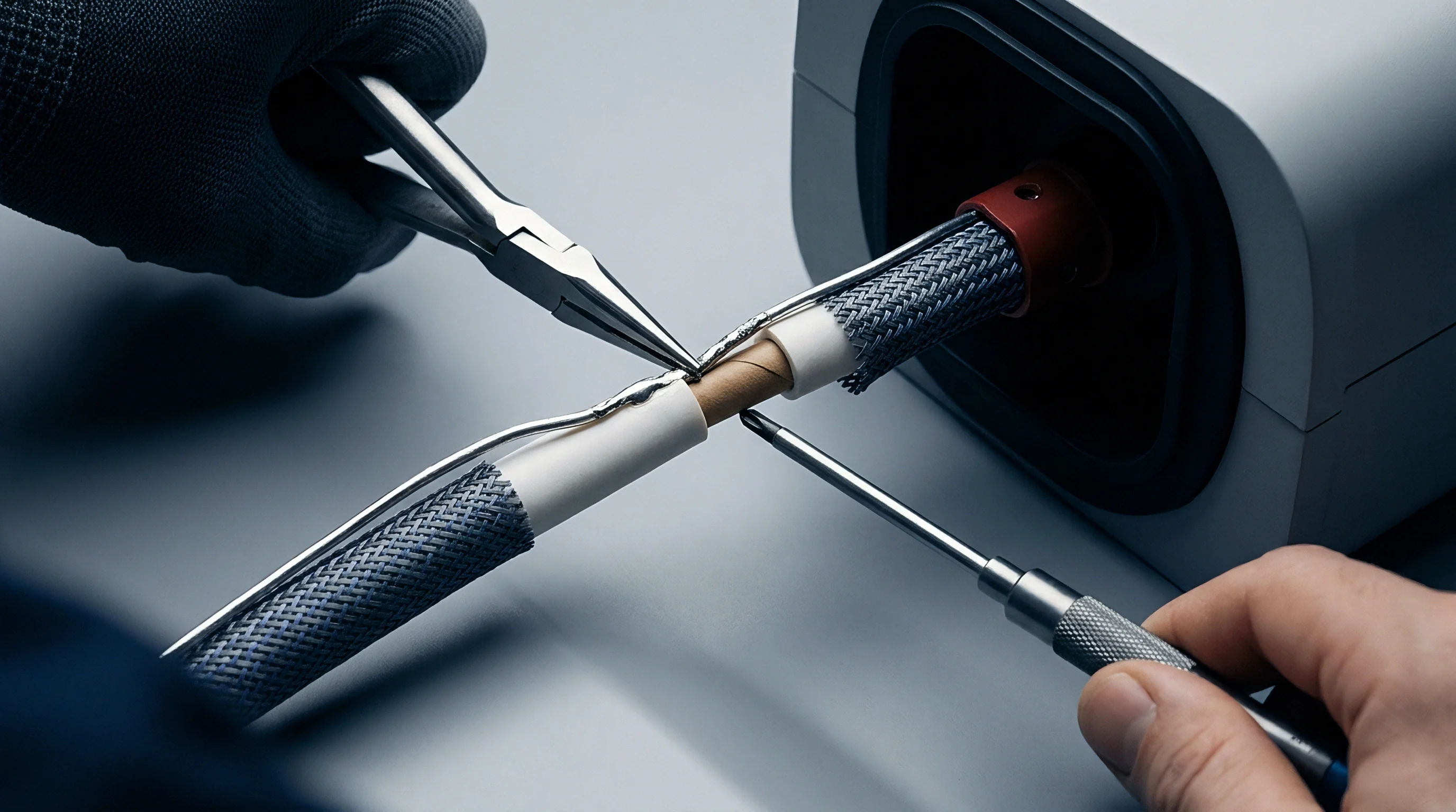
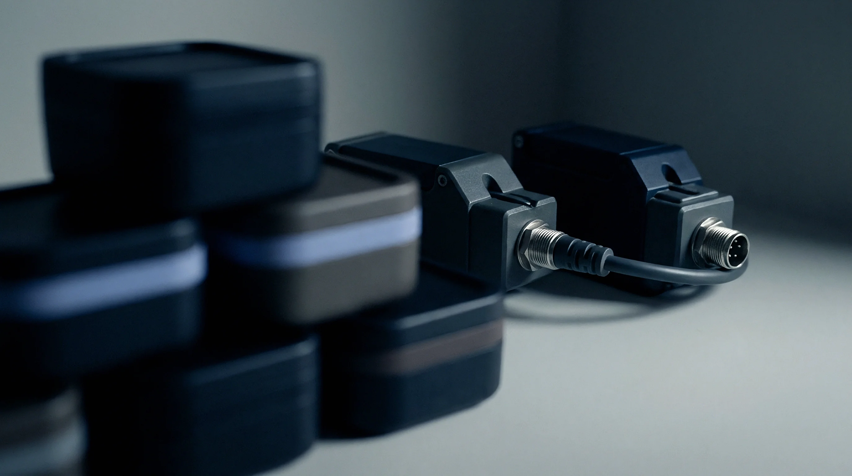
In-line address translation ICs remap seven-bit hardware addresses directly on the wire without software intervention from the host controller. These translators monitor incoming byte streams on the primary bus and alter target address bits on the fly as data crosses to the secondary segment. Modifying the bits in hardware allows identical sensors to operate on a continuous electrical trace without address conflicts.
Translators like the LTC4316 sit physically between the host controller and peripheral sensors. The device captures the start condition and address byte sent by the master, checks the address against hardwired translation offsets, and XORs the target bits before passing the byte downstream, leaving the rest of the payload untouched.

In Line Address Remapping Hardware
Dedicated transceivers intercept start conditions and incoming bytes, using XOR logic to alter selected address bits before forwarding the stream downstream. Offset values are set with passive voltage dividers tied to analog pins on the translator package. A single chip supports up to 127 address translations, removing the need for multiplexing routines in firmware.
Hardware translation allows uninterrupted access to every node on the bus without channel-switching overhead. The host firmware reads the array sequentially through mapped virtual addresses, treating each sensor as an independent peripheral on a shared trace. Bidirectional open-drain circuitry maintains two-way signaling during ACK phases and subsequent byte transfers.
UM10204 section 3.1.10 reserves ten-bit address prefixes, rendering active dynamic address translation mandatory for conflicting multi-channel slave groups.
Where Does Address Translation Fail during Fast Bus Sweeps?
Rapid bus sweeps can bypass internal alias registers when repeated start conditions lack intermediate idle states. Tight, back-to-back reads on high-speed buses prevent edge-detection circuits from resetting internal state machines between frames. If setup and hold times fall below 100 ns, the translation logic can misinterpret repeated start sequences as payload data.
Failure modes in active address aliasing disrupt bus timing and introduce transient voltage offset faults on physical traces.
- Bitwise Translation Collision ~ Dynamic address translation devices mapping identical offset masks convert distinct master frames into identical target addresses on secondary buses.
- Acknowledge Spike Degradation ~ Active translation transceivers driving intermediate ACK pulses generate voltage spikes that violate SMBus low-level input thresholds.
- Voltage Level Incompatibility ~ Unbuffered offset translators operating across mixed 1.8V and 3.3V domains exhibit asymmetrical fall times on data lines.
Adherence to NXP I2C Specification UM10204 Clause 3.1.12 mandates that address translators release SDA lines within 30 ns of SCL fall edges to prevent bus protocol violations.
Timing
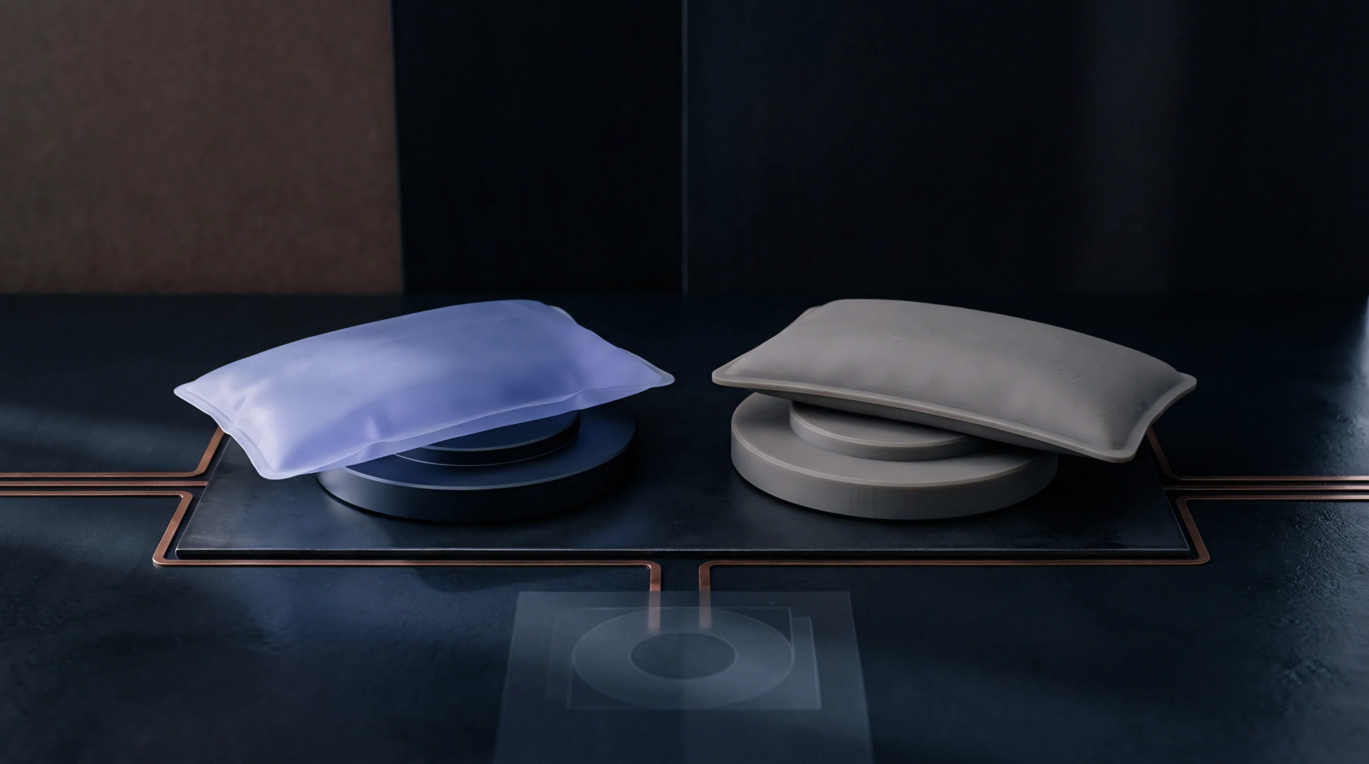
Parasitic trace capacitance builds up with every sensing component added to a two-wire bus. Pin packages, silicon gates, and copper trace lengths all contribute capacitive loading to clock and data lines. This cumulative load slows transition times, rounding off square pulses into exponential RC curves that can violate digital switching thresholds.
Two-wire serial buses rely on open-drain drivers and external pull-up resistors to bring signals high. While active pull-down transistors pull lines low quickly, the low-to-high transition time depends entirely on pull-up resistance and total bus capacitance, which together constrain maximum trace lengths and node counts.
Capacitance Accumulation across Physical Channels
Because bus loading dictates signal slew rates, pull-up resistors must be sized carefully to remain within specification. Standard-mode operation at 100 kHz permits up to 400 pF of bus capacitance. Fast-mode at 400 kHz keeps that 400 pF ceiling but tightens allowable rise times from 1000 ns down to 300 ns.
Fast Mode Plus reaches 1 MHz, requiring rise times under 120 ns against loads up to 550 pF.
Adding environmental sensors over long board runs introduces roughly 10 pF to 25 pF per node. A cluster of sixteen sensors on a single bus can contribute over 300 pF from package pins alone, leaving little capacitive margin for PCB routing.
Higher trace capacitance on extended bus segments demands lower pull-up resistance to satisfy fast mode rise time limits.
Bus Edge Slew and Pull up Calculation
Engineers calculate pull-up resistor boundaries using driver sink current limits for the minimum resistance and rise-time constraints for the maximum. The minimum value keeps the active-low pull-down from exceeding maximum sink currents ~ typically 3 mA for standard parts and 20 mA for Fast Mode Plus. The maximum value treats the line as a first-order RC network, where rise time equals 0.8473 times the pull-up resistance multiplied by total capacitance.
Calculated pull-up resistance values must fall within lower and upper theoretical bounds to guarantee signal rise times match clock frequency requirements.
| Bus Speed Mode | Max Clock Speed | Max Rise Time | Max Bus Capacitance | Nominal Pull-Up Range |
|---|---|---|---|---|
| Standard Mode | 100 kHz | 1000 ns | 400 pF | 2.2 kΩ to 10.0 kΩ |
| Fast Mode | 400 kHz | 300 ns | 400 pF | 1.0 kΩ to 4.7 kΩ |
| Fast Mode Plus | 1000 kHz | 120 ns | 550 pF | 330 Ω to 1.5 kΩ |
| High-Speed Mode | 3400 kHz | 40 ns | 100 pF | Active Current Source |
Clock stretching introduces further timing challenges when slow sensor analog-to-digital converters pull serial clock lines low to pause transactions during data processing cycles. Shortening traces and reducing device count yields cleaner clock edges far more reliably than lowering pull-up resistance on heavily loaded lines.
Transaction
Firmware architectures manage dense sensor buses through structured polling routines that prevent interface hangs. Multi-channel sensors use internal state machines to run conversions, apply factory calibration constants, and set status flags in register banks. Host controllers handle these schedules using non-blocking state machines or RTOS tasks.
System software manages bus bandwidth by grouping sensors into priority queues. Time-critical motion or safety sensors receive frequent polling slots, whereas ambient temperature and environmental monitors update at lower rates. Drivers inspect status registers prior to multi-byte reads, verifying that internal conversions have finished before initiating data transfers.
Polling Schedule and Queue Management
Dense sensor arrays generate asynchronous interrupts that require prioritized buffering on the host. When multiple sensor alert lines share a single open-drain GPIO interrupt pin, triggering an alert forces the host to run rapid register polls across every shared device to identify the source.
Queue starvation occurs when rapid interrupts from fast sensors prevent the controller from servicing slower peripherals. Device drivers address this with fixed ring buffers and round-robin scheduling to balance bus time across nodes. Firmware also runs timeout counters on every transaction to release hung lines if a peripheral fails to acknowledge within a set window.
Unbuffered multiplexer switching events inject transient capacitance shifts directly into host controller timing loops.

Host Driver Architecture Selection
Firmware architects choose between static polling threads and event-driven state machines based on sensor data refresh requirements. Driver selection criteria balance software complexity against real-time bus performance across shared hardware channels.
- Bus Channel Allocation ~ System software checks channel availability before issuing read requests to identical multi-channel address targets.
- Timeout Threshold Configuration ~ Host controllers set bus freeze timers between 25 ms and 35 ms to recover stalled clock lines automatically.
- Interrupt Request Grouping ~ Firmware routing aggregators group shared open-drain interrupt lines into discrete gpio vector tables.
- Broadcast Command Isolation ~ Master drivers isolate multi-channel software resets to single multiplexed downstream channels to avoid resetting operating sensors.
Bus utilization calculations must factor in translation delays, multiplexer switching latency, and sensor register setup times across temperature extremes. Driver overhead increases steadily as node counts rise on a shared physical bus.
Whether future sensor silicon will integrate internal dynamic address negotiation logic without increasing die area or unit cost remains open across the semiconductor industry.
Valuation
Bill-of-materials analysis balances component purchase costs against board space and the software engineering required to support complex bus layouts. Choosing sensors with dedicated address pins raises unit costs slightly but eliminates auxiliary chips. Lower-pin-count variants are cheaper individually, but they force designs to incorporate multiplexers, address translators, or auxiliary host buses.
Component choices carry manufacturing implications beyond the basic BOM. Adding multiplexers or translation chips increases board area, raises component counts, and adds solder joints that can depress assembly yields.

Direct Component Cost Comparison
Sensor variants with dedicated address pins generally carry a three to five percent price premium over minimal pin-count versions. For example, a quad pressure sensor in a QFN-16 package with three address pins costs $1.45 at 10,000 units, whereas the same die in a space-saving DFN-10 package with one address pin costs $1.38 at the same volume.
Adding an eight-channel TCA9548A multiplexer increases BOM costs by $0.42 at 10,000 units, plus roughly $0.06 in surface-mount placement costs for pull-up resistors and decoupling capacitors. An active address translator like the LTC4316 adds $1.85 per channel at comparable volumes. The optimal architecture shifts depending on the number of identical nodes sharing the board.

Total Engineering Effort and Layout Impact
Software development timelines scale significantly when custom driver layers must handle dynamic multiplexer switching and address alias management. Engineering labor costs associated with writing, testing, and qualifying multi-channel bus multiplexing drivers average two to three software development weeks, representing an upfront engineering investment of $8,000 to $12,000.
| Topology Option | Added BOM Cost (10k Units) | Board Area Penalty | Firmware Development Weeks | Total Delivered Cost Threshold |
|---|---|---|---|---|
| Hardware Pin Strapping | $0.00 (Standard) | 0 mm² | 1 Week | Lowest below 4 Nodes |
| Hardware Multiplexing | $0.48 per 8 Channels | 16 mm² | 3 Weeks | Lowest from 5 to 16 Nodes |
| Active Translation | $1.85 per Channel | 9 mm² | 2 Weeks | Niche High-Density Arrays |
| Secondary Master Bus | $0.25 (MCU Pin Cost) | 4 mm² | 2 Weeks | Lowest if Host Micro Exists |
Engineers balancing long-term production costs against upfront firmware integration cycles select multiplexer expansion topologies when multi-channel sensor counts exceed four units on a single board layout.