Differential Pair Impedance Control in High Temperature Sensor Wiring
High-temperature differential pairs maintain 100-ohm impedance by matching thermal permittivity drift with trace spacing expansion tolerances across operating gradients.

Laminate

Dielectric Shift across Elevated Thermal Gradients
High-temperature sensor wiring relies on stable dielectric properties to maintain differential characteristic impedance (Zd). Standard FR-4 laminates undergo catastrophic resin softening and dielectric breakdown above 130°C to 170°C. Applications operating between 200°C and 500°C require engineered dielectric substrates such as woven glass reinforced polytetrafluoroethylene (PTFE), polyimide, ceramic-filled fluoropolymers, or low-temperature co-fired ceramics (LTCC). Relative permittivity (εr) decreases systematically as temperature rises in unfilled fluoropolymers, directly driving characteristic impedance upward.
A differential pair calibrated for 100 Ω at 25°C shifts to 108 Ω or higher at 250°C if dielectric thermal coefficients are ignored during stack-up design.
Thermal expansion along the vertical z-axis alters the dielectric height (h) separating signal traces from reference planes, while expansion in the x-y plane increases trace width (w) and edge-to-edge separation (s). Glass transition temperature (Tg) marks the physical boundary where the coefficient of thermal expansion (CTE) accelerates sharply. Below Tg, polyimide laminates exhibit a z-axis CTE of approximately 45 p±/circC; above Tg, this expansion rate rises to 210 p±/circC.
This non-linear geometric distortion shifts trace dimensions and substrate thickness unevenly, disrupting the capacitive coupling balance between conductors.
Relative permittivity drops from 3.40 at 25°C to 3.12 at 250°C in ceramic-filled PTFE, raising differential impedance by 5.8 Ω in a 100 Ω edge-coupled microstrip.
Edge-Coupled Trace Geometry Calculations
Analytical impedance modeling for high-temperature differential pairs requires evaluating single-ended impedance (Z0) and mutual coupling factor (k) across operational temperature extremes. Consider an edge-coupled microstrip construction on a high-temperature ceramic-filled PTFE substrate. The single-ended characteristic impedance is defined as:
Z0 = frac87sqrtεr + 1.41 lnleft( frac5.98 h0.8 w + t right)
where h is dielectric thickness, w is trace width, and t is copper thickness. Differential impedance Zd incorporates intra-pair spacing s through the coupling coefficient:
Zd ≈ 2 Z0 left( 1 – 0.48 expleft( -0.96 fracsh right) right)
Assume an ambient reference design at 25°C with w = 0.127 mm (5.0 mil), s = 0.127 mm (5.0 mil), h = 0.1016 mm (4.0 mil), and copper weight of 1 oz (t = 0.0355 mm). At 25°C, εr = 3.40, yielding Z0 = 58.2 Ω and Zd = 99.6 Ω. When the assembly operates continuously at 250°C, thermal expansion increases dielectric height h to 0.1058 mm due to z-axis expansion, while trace width expands to 0.128 mm.
Simultaneously, the elevated thermal state reduces εr to 3.12. Re-evaluating the geometry under thermal equilibrium yields Z0 = 61.4 Ω and Zd = 105.4 Ω. This 5.8 Ω deviation creates impedance mismatches at interface connectors, triggering signal reflections that distort sensor telemetry.
| Material Designation | Continuous Rating (°C) | Permittivity at 25°C | Permittivity at 250°C | Z-Axis CTE (ppm/°C) | Differential Drift (%) |
|---|---|---|---|---|---|
| High-Tg Polyimide | 230 | 3.60 | 3.45 | 50 | +4.2 |
| Woven PTFE / Glass | 260 | 2.17 | 2.08 | 135 | +6.8 |
| Ceramic-Filled PTFE | 280 | 3.40 | 3.12 | 42 | +5.8 |
| Alumina Ceramic (96%) | 500 | 9.80 | 9.95 | 7.2 | -0.9 |
Material selections must balance electrical performance with physical durability under operational stress. High-Tg polyimide maintains mechanical stability up to 230°C but absorbs moisture up to 1.3%, which elevates dielectric loss over time. Ceramic-filled PTFE limits z-axis expansion while suppressing dielectric constant changes, making it viable for long-run high-frequency differential sensor links up to 280°C. For turbine exhaust and industrial kiln applications exceeding 300°C, thick-film conductors printed directly on 96% alumina substrates offer superior dimensional stability, limiting total impedance drift within 1.0% across a 400°C thermal span.
IPC-4101E specification sheet 42 establishes thermal expansion limits for high-performance polyimide laminates, requiring z-axis CTE below 60 p±/circC prior to glass transition to prevent micro-via shear and differential trace delamination during high-temperature dwell cycles.
Strand
Conductor Metallurgy and Resistance Escalation
Differential pair impedance depends directly on conductor resistance and cross-sectional stability at elevated temperatures. Standard electrolytic tough pitch (ETP) copper oxidizes rapidly above 150°C, causing surface flaking, loss of cross-sectional area, and permanent shifts in characteristic impedance. High-temperature sensor wiring requires specialized conductor metallurgy, including silver-plated copper, nickel-plated copper, and 27% nickel-clad copper.
The electrical resistivity (ρ) of annealed copper rises from 1.72 × 10⁻⁸ Ω·m at 20°C to 3.28 × 10⁻⁸ Ω·m at 250°C, governed by the temperature coefficient of resistance (α = 0.00393 / circC):
ρ(T) = ρ0 left
High DC resistance increases series attenuation (αd), reducing the signal magnitude reaching the host receiver. At high frequencies, skin depth (δ) dictates where current flows within the conductor cross-section:
δ = sqrtfracρπ f μ0 μr
Because resistivity ρ increases with heat, skin depth expands at elevated temperatures. In nickel-plated conductors, the high magnetic permeability (μr ≈ 100 to 600) and high bulk resistivity of nickel (6.9 × 10⁻⁸ Ω·m) restrict high-frequency signal currents to the thin outer plating layer, creating non-linear insertion loss profiles across temperature sweeps.
Conductor plating thickness stability governs high-temperature attenuation far more than trace geometry tolerances.
High-temperature environments introduce specific degradation pathways in differential pair conductors that destroy signal integrity if left unmanaged:
- Nickel Interdiffusion causes copper atoms to migrate through thin nickel plating at temperatures exceeding 200°C, forming resistive surface oxides that elevate high-frequency insertion loss.
- Silver Migration creates conductive filament paths across insulation material under high humidity and continuous DC voltage bias, inducing inter-pair leakage currents.
- Thermal Grain Growth weakens fine-gauge solid conductors subject to mechanical vibration, causing work hardening and fatigue fractures at sensor termination housings.
- Differential Diameter Variance introduces physical asymmetry between the two conductors of a pair, converting differential signals into destructive common-mode noise.
Twisted-Pair Cable Geometry under Stress
In cabled sensor harnesses, differential impedance relies on tight geometric control of conductor center-to-center distance (D) and wire diameter (d). Characteristic impedance for a shielded twisted pair (STP) cable is calculated via:
Zd = frac120sqrtεr lnleft( frac2 Dd frac1 – σ21 + σ2 right)
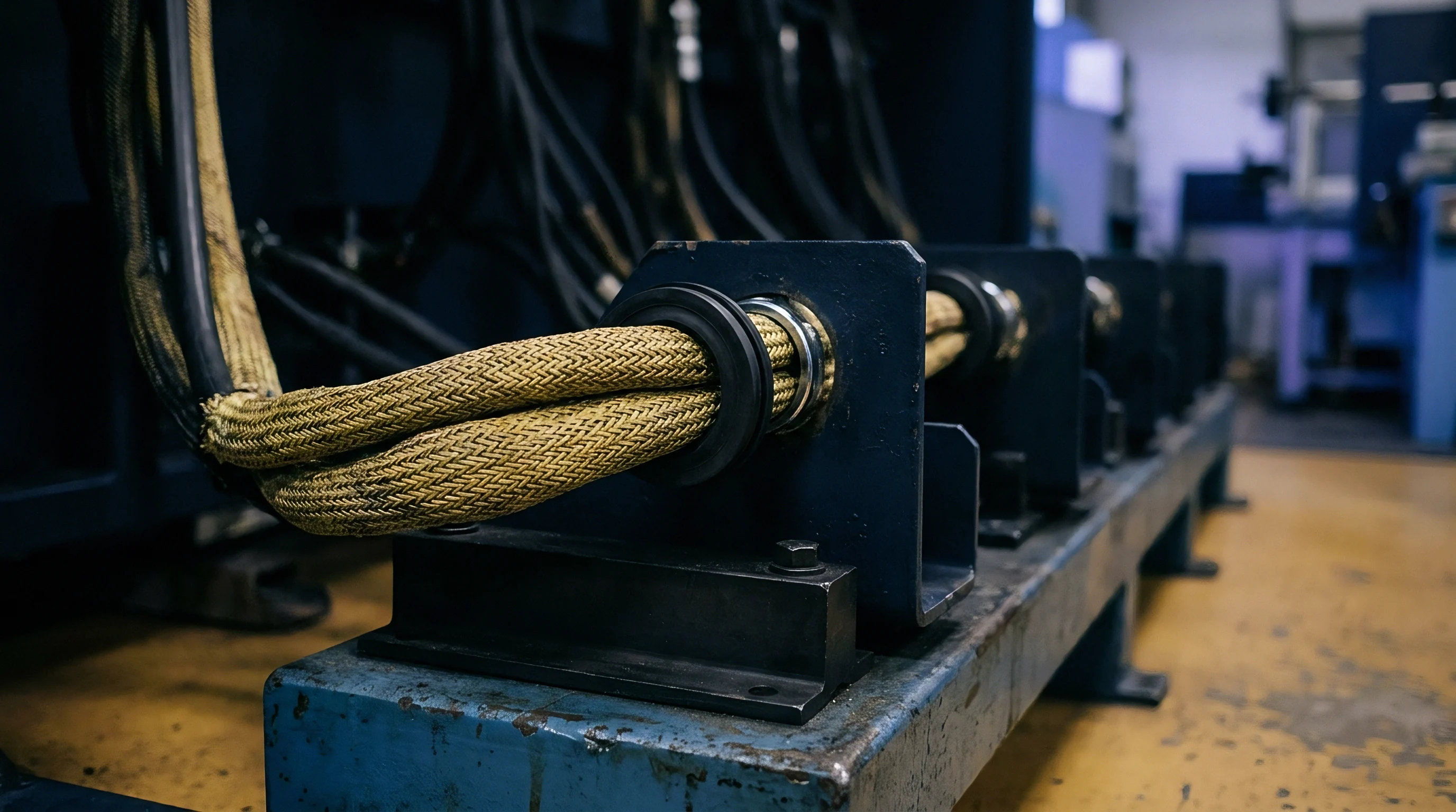
where σ = D / (2 hs) and hs represents the distance to the outer shield. Mismatched mechanical expansion between fluoropolymer insulation and metal conductors alters D along the cable length. When flexible sensor wires experience bending stresses at 200°C, soft insulation materials compress at contact points, decreasing conductor spacing D and causing localized drops in differential impedance down to 82 Ω.
Plating thickness variations across production batches may fall within standard ASTM B355 allowances, yet batch-to-batch plating tolerances introduce up to 4.5 Ω of impedance variance across high-temperature operational runs.

Skew
Which Dielectric Parameter Drives Impedance Shift at High Temperature?
Anisotropic thermal expansion within reinforced dielectric laminates drives intra-pair skew and impedance shifts at high temperatures. Reinforced substrates use woven glass fabrics embedded in resin matrix materials. Glass fibers (E-glass CTE of 5.4 p±/circC) expand at a drastically lower rate than the surrounding polymer matrix (50 to 130 p±/circC).
When one leg of a differential pair sits directly over a glass bundle cross-over while the twin leg sits over a resin-rich pocket, thermal expansion spreads the two conductors unevenly. Relative permittivity experienced by the first conductor remains stable, whereas permittivity around the second conductor drops rapidly as the resin heats. This local dielectric disparity creates phase velocity mismatches along the pair.
Phase delay (τ) per unit length is defined as:
τ = fracsqrtεeffc
where c is the speed of light in vacuum and εeff is the effective dielectric constant. A permittivity imbalance (Δ εeff) between conductors converts clean differential signals into common-mode noise. Skew accumulation (Δ tskew) over length L follows:
Δ tskew = fracLc left( sqrtεeff1 – sqrtεeff2 right)
At 250°C, a 0.5-meter sensor lead with a 5% dielectric imbalance produces over 120 picoseconds of intra-pair skew. For a 500 Mbps differential sensor interface (such as high-speed SPI or RS-485 variants running over cabled interconnects), 120 picoseconds consumes over 12% of the total bit period, collapsing the timing margin at the receiver input.
A 5% permittivity imbalance between twin conductors over a 0.5-meter high-temperature lead produces 120 picoseconds of skew, consuming 12% of the bit window at 500 Mbps.
Termination Resistor Drift and Mode Conversion
Differential lines mandate matched parallel termination (RT = Zd) at the receiver end to prevent signal reflections. Thick-film chip resistors suffer from temperature coefficients of resistance (TCR) ranging from ± 100 to ± 300 p±/circC. A standard 100 Ω thick-film resistor operating across a 200°C thermal rise shifts in value by up to ± 6 Ω.
Thin-film precision metal film resistors limit TCR to ± 10 or ± 25 p±/circC, keeping thermal drift under 0.5 Ω.
When termination resistance strays from characteristic line impedance, differential reflection coefficient (Γd) increases:
Γd = fracRT – ZdRT + Zd
Mode conversion parameters (Scd21) quantify how much differential signal energy transforms into common-mode noise due to termination drift and line asymmetry. High common-mode noise degrades signal-to-noise ratio (SNR), causing bit error rates (BER) to spike in hostile automotive, aerospace, and industrial environments.
Failing to match dielectric thermal coefficients and line termination drift converts differential telemetry into common-mode noise, swamping receiver inputs and causing sensor communication outages across thermal ramp-up cycles.
Audit
Time-Domain Reflectometry under Thermal Dwell
Evaluating differential impedance control in high-temperature sensor assemblies requires Time-Domain Reflectometry (TDR) performed inside environmental test chambers. High-frequency TDR pulses (rise times $
Bench testing requires systematic procedures to isolate board-level dielectric shifts from cable connector degradation during thermal sweeps, preventing signal reflections from distorting telemetry readings:
- Connect phase-stable thermal extension cables rated to 250°C between the TDR instrument ports and the environmental test chamber bulkhead.
- Perform a full short-open-load-thru (SOLT) differential calibration at room ambient (25°C) to set the reference baseline plane at the chamber bulkhead.
- Place the sensor wiring harness and PCB substrate assembly inside the chamber, securing signal terminations to high-temperature precision 2.92 mm or SMA launch connectors.
- Ramp the chamber temperature at 5circC/min to the maximum operating ceiling, holding isothermal soak points every 50°C for 30 minutes to allow dielectric equilibration.
- Record TDR differential impedance profiles, insertion loss (Sdd21), and return loss (Sdd11) at each temperature plateau using a vector network analyzer.
| Location Point | Test Temp (°C) | Measured Zd (Ω) | Physical Mechanism | Severity Assessment |
|---|---|---|---|---|
| Launch Connector | 250 | 93.2 | Dielectric expansion in SMA insulator | Moderate reflection |
| PCB Microstrip | 250 | 106.1 | Substrate permittivity decay (εr downarrow) | In tolerance ($ |
| Harness Splice | 250 | 84.5 | Solder joint displacement / conductor nip | Critical impedance dip |
| Sensor Head Termination | 250 | 101.8 | Thin-film resistor TCR drift | Low impact |
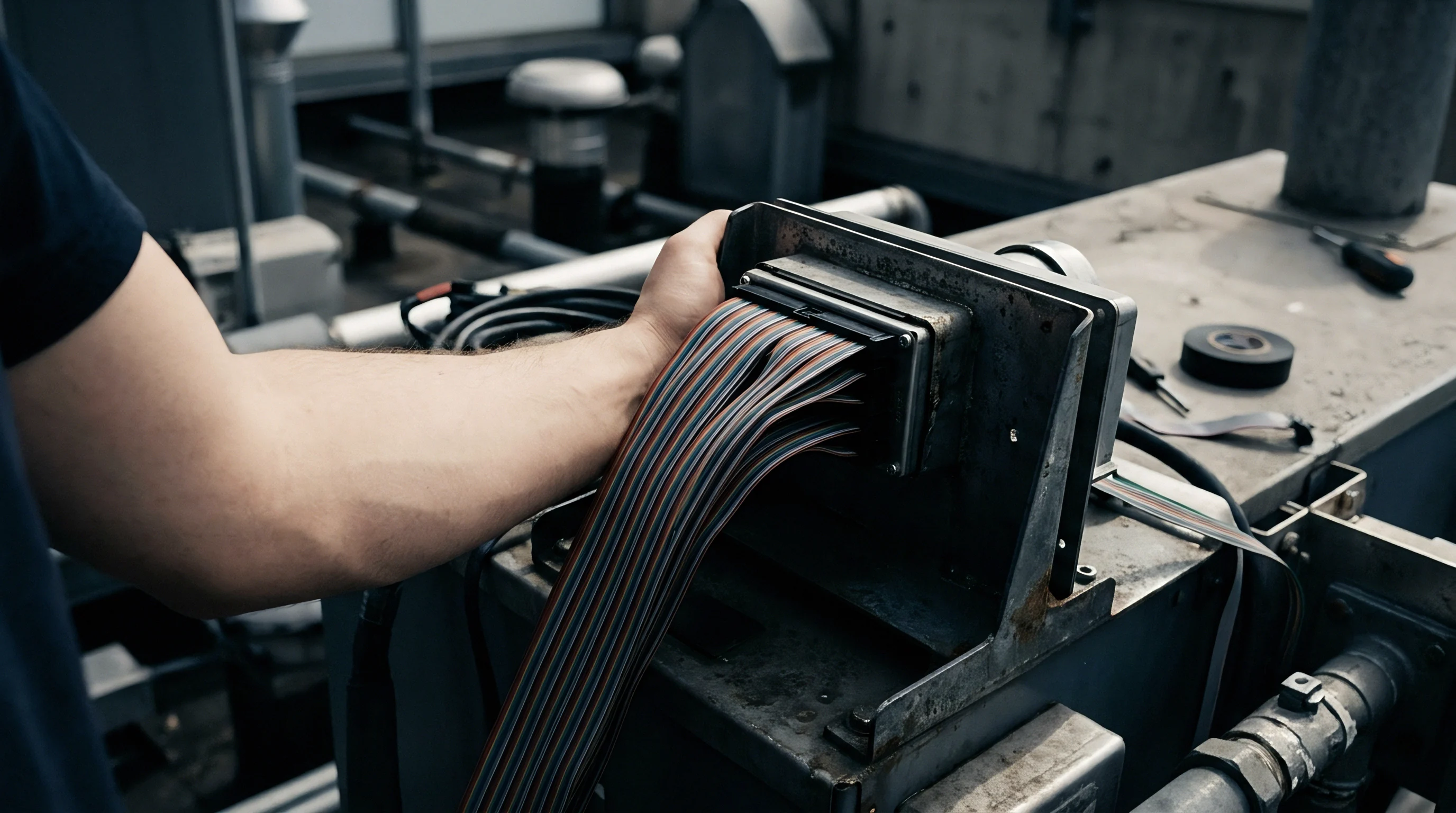
Discontinuities recorded during heat sweeps pinpoint physical failure points. A sharp impedance drop at a harness splice indicates mechanical deformation of the wire insulation or solder flow under thermal load. Conversely, a gradual upward slope across the microstrip trace confirms substrate permittivity decay as heat permeates the laminate structure.
Cold measurements disguise thermal drift.
High-temperature TDR verification reveals whether micro-cracking within ceramic-filled PTFE matrices during cyclic thermal stress permanently alters characteristic impedance beyond self-calibration capability.
Yield
Commercial Variant Selection and Integration Arithmetic
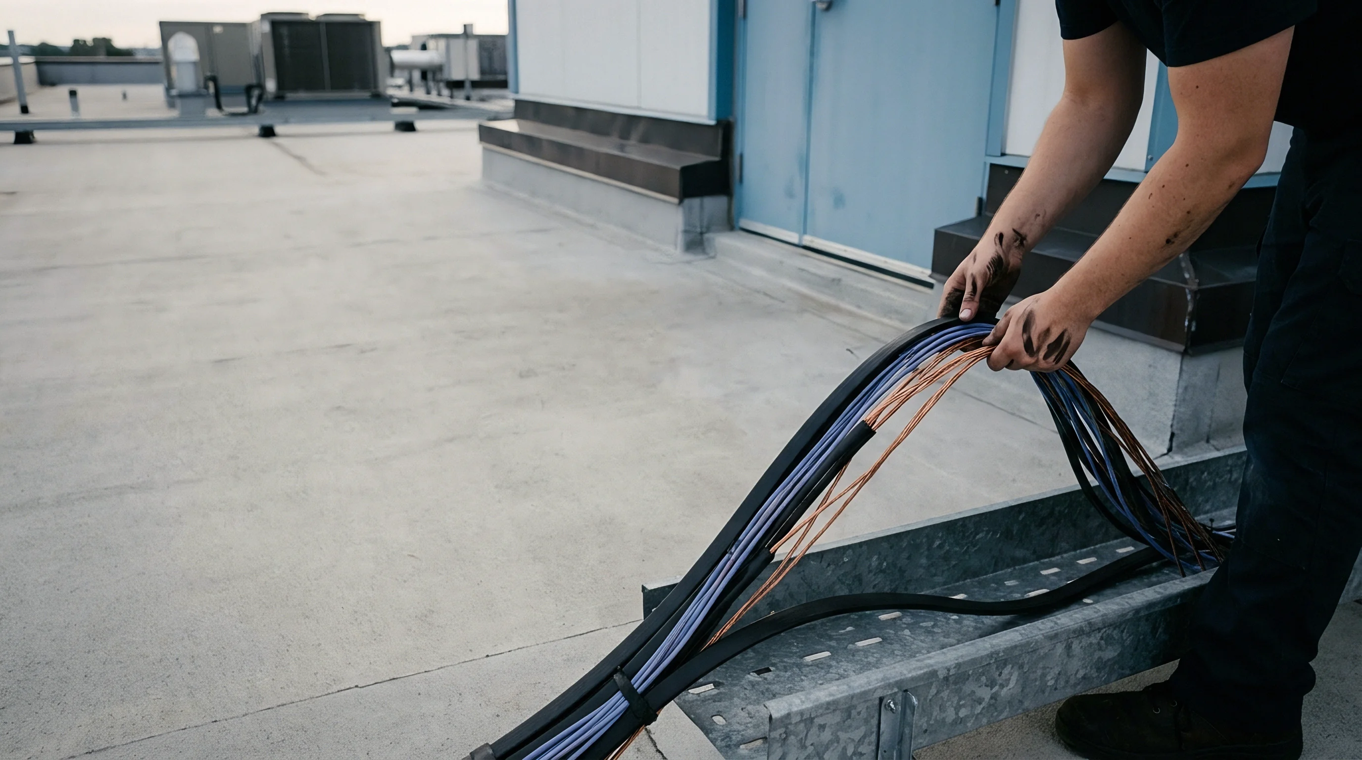
Selecting the optimal physical form factor for high-temperature differential sensor wiring requires balancing unit purchase cost, PCB real estate, assembly yield, and non-recurring engineering (NRE) tooling charges. One underlying sensor die can reach a product build in five distinct variants: a bare surface-mount (SMD) package, an embedded substrate module, a potted ceramic carrier, a mineral-insulated (MI) cabled probe, or an integrated stainless-steel housed transmitter assembly.
Make-or-buy decisions hinge on production volume and internal assembly capabilities. Building a high-temperature differential harness in-house demands specialized crimping tools, automated twisting machines, and braze-inspection equipment. High temperatures accelerate conductor oxidation.
Yield losses on high-temperature surface-mount reflow lines running specialized lead-free solders (e.g. Au80Sn20 with melting point at 280°C) often reach 8% to 12% during initial ramp-up. Sourcing pre-tested, factory-calibrated cabled probes transfers assembly yield risks directly to the harness vendor.
| Variant Package Form | Unit Cost @ 1k (USD) | Reflow / Braze Yield (%) | NRE Tooling (USD) | Firmware Bring-Up (Weeks) |
|---|---|---|---|---|
| Bare SMD Package (DFN) | $4.20 | 91.5 | $2,500 | 4 |
| Embedded LTCC Carrier | $12.80 | 96.2 | $8,000 | 3 |
| Potted Ceramic Module | $28.50 | 98.0 | $4,500 | 2 |
| Mineral-Insulated Probe Wire | $64.00 | 99.1 | $12,000 | 1 |
| Housed Stainless Transmitter | $145.00 | 99.8 | $0 | 1 |
The total landed cost per installed unit (Ctotal) incorporates component price (Ccomp), direct assembly labor (Clabor), amortized NRE tooling (NRE / V), and yield loss penalty (Y):
Ctotal = fracCcomp + ClaborY + fracNREV
Assume a design requirement for 2,000 high-temperature pressure sensor nodes operating at 250°C. Choosing a bare SMD solution on a custom high-Tg polyimide PCB yields Ccomp = 4.20, Clabor = $6.50, NRE = $2,500, and Y = 0.915. The landed unit cost calculates to:
$Ctotal, SMD = frac4.20 + 6.500.915 + frac25002000 = $11.69 + $1.25 = $12.94
Alternatively, specifying a pre-assembled mineral-insulated cabled probe eliminates board-level high-temperature reflow processing, yielding $Ccomp = $64.00, Clabor = $1.20, NRE = $12,000, and Y = 0.991. Landed unit cost calculates to:
$Ctotal, MI = frac64.00 + 1.200.991 + frac120002000 = $65.79 + $6.00 = $71.79
At 2,000 units, the bare SMD route saves $58.85 per node in direct material and tooling costs. However, if firmware bring-up and qualification testing reveal high common-mode noise issues caused by uncompensated board-level thermal drift, fixing the design requires an additional PCB iteration ($3,500) and four engineering weeks ($16,000), consuming the material savings achieved across 330 production units.
Contractual RFQ documentation for high-temperature differential pair harnesses demands exact specification clauses to protect delivery schedules and unit yields:
- Dielectric Permittivity Bounds dictate maximum allowable εr deviation across the specified operating temperature range (e.g. Δ εr le ± 0.15 from 25°C to 250°C).
- Intra-Pair Length Matching mandates mechanical wire cutting tolerances held within ± 0.1 mm to prevent phase skew accumulation.
- High-Temperature Burn-In requires 100% pre-shipment thermal cycling at maximum rated temperature for 24 hours to stabilize conductor stress and outgas volatile compounds.
- TDR Impedance Acceptance enforces 100% test logging verifying differential impedance remains within 100 ± 7.5 Ω across the thermal profile.
Target differential impedance tolerances set at ambient temperature must be halved if the operational harness spans distinct thermal zones.