Microvia in Pad Planarization Effects on High Density PCB Signal Integrity
Microvia pad planarization eliminates solder joint voids and stabilizes high-frequency trace impedance by controlling dimple depth and copper cap topography.
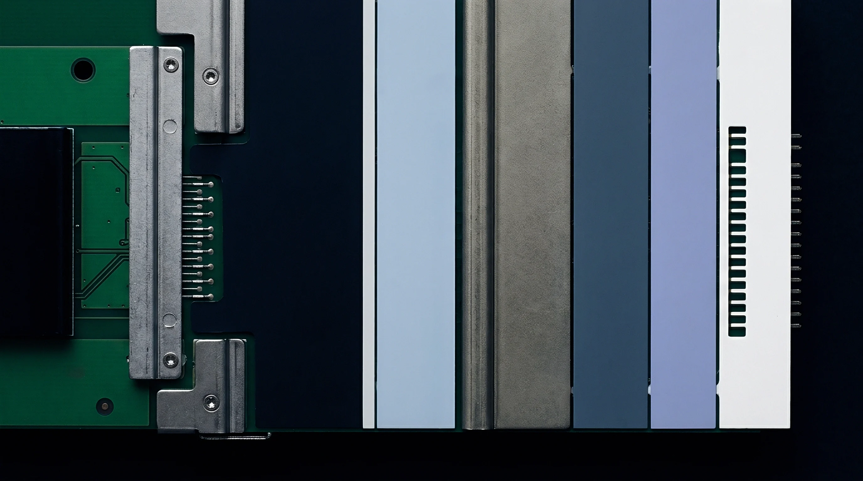
Topography
Laser-drilled microvias landing on high-density interconnect layers change the surface profile of component pads. When an interconnect sits directly inside a ball grid array land pattern, any depression or protrusion dictates where the solder sphere wets. Whether the joint forms a true planar interface or draws solder down into a central pocket depends entirely on the copper cap over the filled cavity.
Dimensional control here directly affects high-frequency propagation: profile deviations distort reference return paths, introduce localized capacitive discontinuities, and disrupt transmission line impedance across the outer layers.
Electroplating bath chemistry, leveler performance, and downstream mechanical finishing all dictate the final pad profile once copper bridges the laser-drilled hole. Without secondary planarization, an electroplated via-in-pad tends to leave a measurable dimple. Conversely, baths run with excess metal to guarantee hole fill often leave a raised bump.
Either variation compromises the uniform standoff needed between the copper land and the mating solder ball.
| Topographical Metric | Standard Non-Planar Fill | Controlled Chemical Fill | CMP Planarized Cap | IPC-6012 VI Specification |
|---|---|---|---|---|
| Dimple Depth (Recession) | 12 to 25 μm | 5 to 10 μm | 0 to 2 μm | Maximum 7.6 μm |
| Bump Height (Protrusion) | 15 to 30 μm | 6 to 12 μm | 0 to 1.5 μm | Maximum 5.0 μm |
| Copper Cap Thickness | 10 to 18 μm | 12 to 22 μm | 15 to 25 μm | Minimum 12.0 μm |
| Surface Roughness (Ra) | 0.45 to 0.70 μm | 0.35 to 0.50 μm | 0.12 to 0.25 μm | Unspecified |
| Land Coplanarity Variance | ±12 μm | ±6 μm | ±1.5 μm | ±5.0 μm |
Under IPC-4761, Type VII covers filled and capped vias completely plugged with resin or copper and sealed with a planarized metal cap. Holding coplanarity across fine-pitch arrays remains difficult for board shops. At 0.4 mm and 0.35 mm pitches, pad diameters shrink to 220 μm or smaller, forcing microvia targets below 100 μm where any dishing in the cavity readily pulls in solder paste.
Such dimples shift the localized capacitance of the pad.
- Dishing depressions pull liquid solder from the joint periphery during reflow, leaving central micro-voids that displace conductive alloy.
- Protruding copper domes lift the stencil off the board during printing, smearing paste across adjacent ultra-fine-pitch pads.
- Recessed land margins introduce step transitions that disrupt the return-current distribution across the conductor surface.
- Chemical leveler residues lodged in steep via crevices inhibit uniform intermetallic growth between copper and tin-silver-copper alloys.
Uniform solder volume depends on a planar surface. Chemical-mechanical planarization or careful mechanical polishing yields pads with elevation differences held under two micrometers. Because signals above twenty gigahertz travel primarily through the outer few hundred nanometers of conductor, geometric irregularities alter the phase constant and create micro-reflections that erode timing margins.
Flat pads also ensure consistent paste release during stencil printing.
Cap
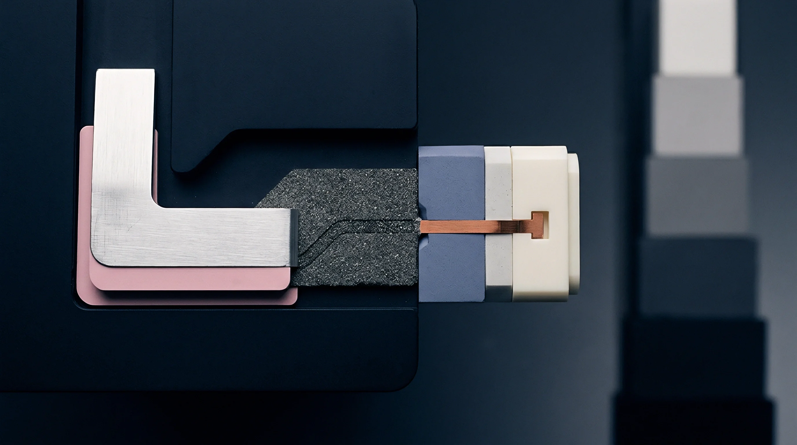
Sequential Metallization and Planarization Stages
Secondary finishing turns an uneven electroplated fill into a flat land. Once laser ablation cuts through the outer dielectric to reach the capture pad on layer two, desmear chemistry cleans and conditions the hole wall. Direct metallization follows, laying down either thin electroless copper or a conductive seed layer before acid copper plating with suppressors, accelerators, and levelers.
Suppressors adsorb onto the outer pad to slow deposition, while accelerators gather at the base of the via to drive bottom-up growth. Levelers target high-shear rim edges to prevent overplating. When additive concentrations drift out of balance, the bath either underfills the hole into a pronounced dimple or plates out runaway nodules into high bumps, yielding thin copper caps that crack under thermal stress.
A four-micrometer dimple depression on an eighty-micrometer microvia land reduces signal propagation velocity by two percent at twenty-eight gigahertz.
Mechanical sanding or chemical-mechanical polishing strips back the plated copper overburden across the panel. Fabricators run boards through multi-head scrubbers fitted with non-woven abrasive wheels or diamond slurry belts, using abrasive pads to cut down high peaks. Chemical-mechanical planarization couples this mechanical abrasion with chemical etching, leveling the copper cap flush with the surrounding laminate.
- Laser hole formation cuts through the dielectric with an ultraviolet or carbon dioxide beam, maintaining an aspect ratio typically around 0.8:1 to prevent plating shadows.
- Superfilling electrodeposition relies on differential additive diffusion for bottom-up copper growth, leaving an overburden layer across the surface as the core seals.
- Mechanical abrasion knocks down copper peaks with graded silicon carbide rolls to establish baseline panel uniformity.
- Chemical planarization etches the surface in an abrasive slurry suspension, leaving the pads flat and flush with the surrounding mask baseline.
- Barrier cap plating deposits an electrolytic or chemical copper wrap to meet IPC Class 3 minimum foil thickness requirements.
Resin-filled microvias require a different route: the shop drills the blind hole, deposits electroless copper along the barrel, and squeegees non-conductive epoxy paste into the cylinder. Because thermal curing shrinks the resin plug, a mechanical planarization step must grind away any protruding epoxy before an additional plating pass seals the exposed plug with a secondary copper cap. Over-polishing here thins the surface copper, leaving areas prone to high resistance and poor peel strength.
While slight surface dimples may fall within standard visual limits, they nonetheless cause paste volume loss during fine-pitch stencil printing.
Reflection
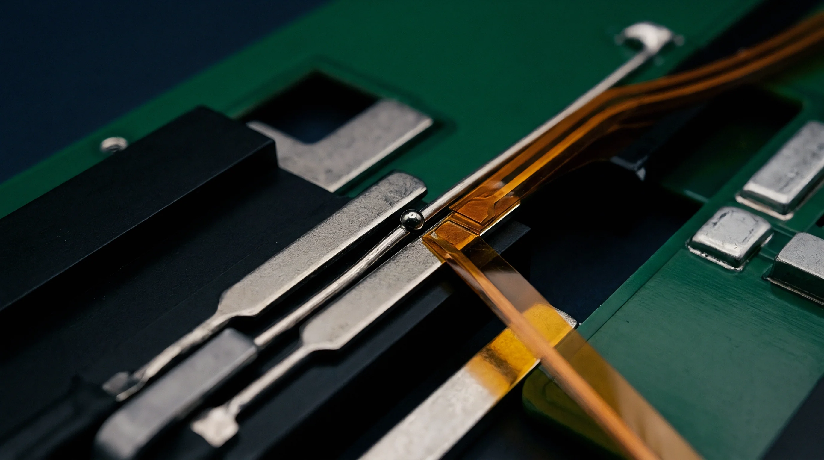
Do Dimple Depressions Degrade Return Loss?
Any abrupt physical transition along a high-frequency conductor creates an electromagnetic discontinuity. On serial channels running at 56 Gbps and 112 Gbps PAM4, loss budgets leave little margin for error. Placing a microvia directly in a pad introduces both a geometric cavity and a localized stub, with cavity dishing introducing parasitic inductive stubs.
Impedance drops noticeably at the via transition. As a signal passes from the component solder sphere through an unplanarized microvia into an escape trace, the dimple increases the physical gap to the ball and alters the conduction perimeter. When reflowing solder fills this depression, the added conductive volume introduces excess capacitance, pulling the characteristic impedance three to eight ohms below the nominal fifty-ohm target.
| Topography State | Nominal Impedance | TDR Dip (Zmin) | Return Loss S11 at 14 GHz | Return Loss S11 at 28 GHz |
|---|---|---|---|---|
| Flat CMP Planarized | 50.0 Ω | 49.1 Ω | -28.4 dB | -21.2 dB |
| 5 μm Recessed Dimple | 50.0 Ω | 46.8 Ω | -22.1 dB | -16.4 dB |
| 15 μm Recessed Dimple | 50.0 Ω | 42.3 Ω | -17.5 dB | -11.8 dB |
| 8 μm Overfill Protrusion | 50.0 Ω | 47.5 Ω | -24.3 dB | -18.0 dB |
| Solder-Starved Dimple Void | 50.0 Ω | 54.6 Ω | -16.2 dB | -10.5 dB |
Because differential signaling relies on tightly matched positive and negative lines, asymmetric pad profiles extract a heavy penalty at high frequencies. When differential pairs enter dense pin fields, microvias often sit directly on adjacent lands. If one pad has a twelve-micrometer dimple while its mate is planarized, the physical asymmetry immediately unbalances the pair.
Coplanar pad surfaces without dimples maintain balanced capacitive loading across differential channel pairs.
Intra-pair skew across this transition zone triggers common-mode noise conversion as phase delays diverge. With mismatched reflection coefficients, signal energy bounces back and forth between the solder ball interface and the first reference plane change.
Energy reflected back toward the transmitter closes the vertical eye margin. In time-domain reflectometry, these impedance dips show up as sharp capacitive notches right at the board interface, and S-parameter data shows return loss degrading steeply once dimple depths exceed five micrometers at frequencies above fifteen gigahertz.
- Capacitive loading dips occur when excess solder pools in deep dimples, pulling line impedance down toward forty ohms.
- Inductive discontinuity spikes arise when trapped flux residue or outgassing prevents wetting, leaving voids beneath the solder sphere.
- Mode conversion generation turns differential energy into radiating common-mode emissions as physical asymmetries ruin phase balance.
- Impedance ripple amplification burdens receiver equalizers, consuming adaptive DSP margin in the physical-layer silicon.
Failing to maintain planar microvia lands in dense breakout regions pushes channel return loss outside specification, ultimately driving links into high bit error rates and packet drops.
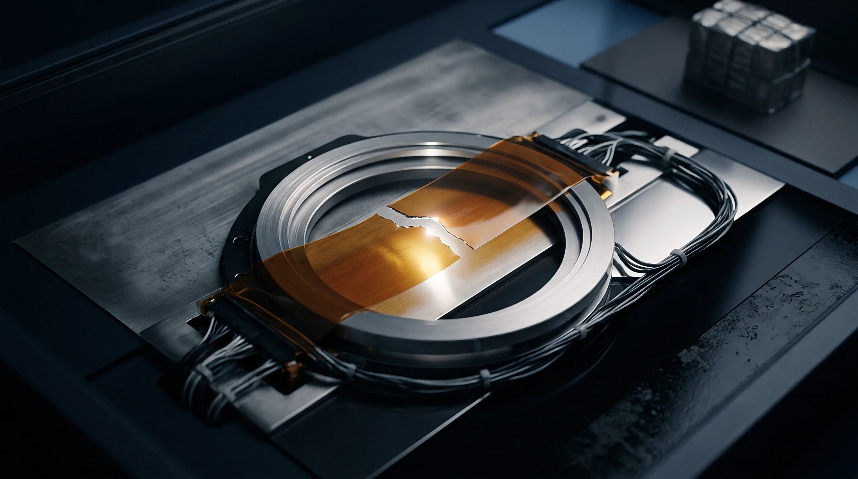

Loss
Are Planar Overfill Bumps Distorting High Frequency Transmission?
Insertion loss accounts for both dielectric absorption and conductor loss along the trace. In dense multilayer boards, skin effect concentrates signal current near the conductor surface; at twenty-eight gigahertz, copper skin depth drops to roughly 0.38 μm. Current crowds almost entirely into the outermost skin of the microvia cap and the trace neck leading away from it.
Mechanical scouring methods used on standard boards cut distinct micro-grooves into the copper foil. While that tooth profile helps solder mask adhere, it disrupts current paths and increases dielectric loss by lengthening the electrical distance across the land. Chemical-mechanical planarization limits this roughness, bringing the arithmetic mean deviation of the profile down below 0.2 μm.
IPC-6012 Class 3 contracts impose a maximum allowable dimple depth of 7.6 micrometers on microvia-in-pad structures to prevent solder ball voiding.
Raised copper mounds create their own high-frequency reflection issues. When prepreg layers are pressed during sequential lamination, bumps squeeze the dielectric thin over the pad, increasing capacitance to the internal reference plane. That localized capacitance bleeds energy from the signal wavefront, dissipating it into the hydrocarbon or polyphenylene oxide resin system.
| Topographical Finish | Dielectric Gap Beneath Pad | Attenuation at 10 GHz | Attenuation at 28 GHz | Phase Delay Skew |
|---|---|---|---|---|
| Fully Planarized (Ra 0.15 μm) | 50 μm nominal | -0.42 dB/in | -1.15 dB/in | 142 ps/in |
| Mechanical Sanding (Ra 0.65 μm) | 48 μm nominal | -0.58 dB/in | -1.62 dB/in | 149 ps/in |
| Convex Bump (10 μm protrusion) | 40 μm localized | -0.72 dB/in | -1.98 dB/in | 158 ps/in |
| Concave Dimple (12 μm depression) | 52 μm localized | -0.64 dB/in | -1.74 dB/in | 152 ps/in |
High-speed serial architectures assume predictable channel transfer characteristics. Discontinuities at the pad transition can set up small standing waves inside the via structure, causing sharp resonant dips in S21. When microvias are stacked across three or four layers, dimples on inner lands compound, generating cumulative phase errors that translate into substantial jitter at the receiver.
Whether secondary plating interfaces within planarized pads introduce measurable skin-effect losses at one hundred gigahertz remains an open question.
Settlement
Procurement specifications continually balance board yield against electrical tolerances. Calling for chemical-mechanical planarization adds twenty-five to forty percent to bare-board pricing compared to conventional filled-and-capped vias, while the extra plating and scrubbing cycles lengthen lead times.
Planarization adds substantial processing overhead: chemical etchback, multi-stage slurry polishing, ultrasonic wash cycles, and frequent cross-sectional checks. Yet when microvia lands drift outside coplanarity tolerances, assembly lines pay for it immediately during reflow. A 0.4 mm pitch ball grid array requires uniform solder volume across every pad in the array; recessed pads starve outer joints, while crowned pads cause bridges between adjacent lands.
| Process Technology | Fabrication Yield | Relative Panel Cost | SMT Assembly Yield | Maximum Signal Rate |
|---|---|---|---|---|
| Standard Mechanical Fill | 88 to 92 % | 1.00 × baseline | 96.2 % | 12.5 Gbps |
| Controlled Leveler Electroplate | 82 to 86 % | 1.18 × baseline | 98.4 % | 28.0 Gbps |
| CMP Planarized Type VII | 72 to 78 % | 1.38 × baseline | 99.7 % | 112.0 Gbps PAM4 |
| Stacked Non-Planar Via | 65 to 70 % | 1.45 × baseline | 94.1 % | 16.0 Gbps |
High-density panels undergoing sequential lamination accumulate thermal stress with each press cycle. Because planarization polishes away outer foil, it reduces panel stiffness; if polishing pressure varies across the working area, the resulting foil imbalances cause bow and twist during lead-free reflow cycles that peak at 260 degrees Celsius, compromising placement accuracy.
Trapped air in deep dimples causes assembly yield to collapse.
Bare board supply agreements specify IPC-A-600 Class 3 acceptance criteria to enforce microvia cap coplanarity limits before assembly release.
Board procurement costs rarely reflect true landed manufacturing economics. Buying cheaper panels with uneven microvia dimples simply shifts scrap and rework costs to the surface-mount line. When x-ray inspection detects voids beneath critical solder spheres, technicians must rework or scrap expensive application-specific integrated circuits and processors.
To guard against this, supply agreements enforce IPC-6012 section 3.6.2.11, rejecting lots where cap recession exceeds five micrometers.