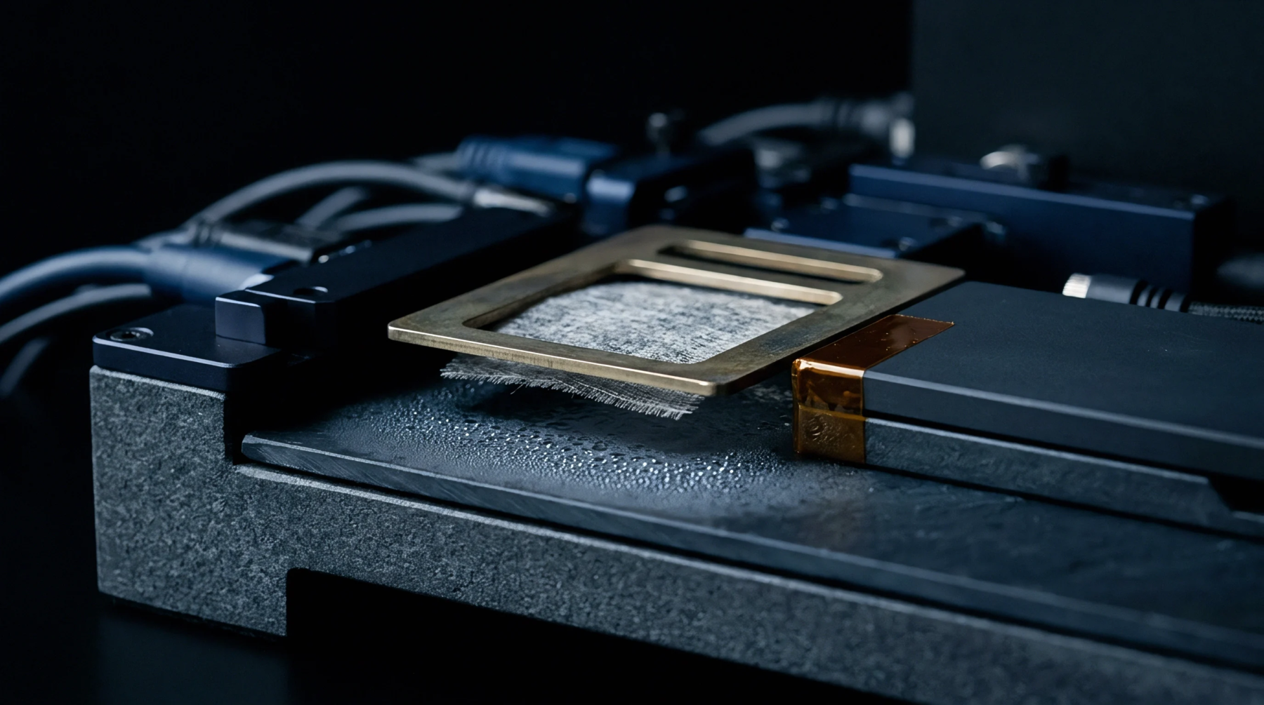
Surface Alignment
Geometric variation between multiple points on the same plane must be minimized to ensure proper joint formation during electronic assembly. This physical alignment characteristic is coplanarity, which defines the maximum distance between the lowest and highest contact points of a component. It determines how well the terminals sit on the solder paste during reflow.
A lack of uniform contact can lead to open circuits.
Assembly Consequence
When component leads or solder spheres are out of plane, some will not touch the circuit board pads during the reflow process. Unconnected pads create electrical open circuits or weak solder joints that fail prematurely. This mechanical separation also causes uneven stress distribution on the remaining pins.
Heavy components can tilt when the plane is uneven, causing solder bridges on the low side. In cases with fine-pitch devices, even a tiny deviation can result in major defect rates during production runs. This means that a deviation of just eighty micrometers can result in incomplete wetting and subsequent field returns.
Measurement Protocol
Specialized automated optical inspection tools measure the relative height of each terminal using laser triangulation or 3D structured light. These systems scan the underside of the package to calculate the least-squares reference plane. The height of every pin or sphere is measured against this computed reference.
Systems flag any parts that exceed the acceptable height variance.
Tolerance Window
Industry standards specify the maximum allowable height deviation for different package styles and lead pitches. Typical values range from fifty to one hundred micrometers depending on the component size. This variation is verified at the end of the manufacturing line before packaging.
Manufacturers calibrate their handling equipment to prevent bending the delicate leads during final tray packing.