Quantifying Heavy Hole Band Degeneracy and Parasitic Leakage Currents in Micro-Machined Pressure Transducers
Dielectric trench isolation on SOI wafers eliminates junction leakage currents, maintaining piezoresistive pressure transducer accuracy above 200°C.


Strain
In un-strained single-crystal silicon, the valence band maximum situated at the Gamma point exhibits six-fold degeneracy when accounting for carrier spin. Mechanical deformation applied to a micro-machined diaphragm lifts this electronic degeneracy. Anisotropic stress breaks the cubic symmetry of the silicon crystal lattice, splitting the heavy hole and light hole energy bands at the wavevector origin.
P-type piezoresistive pressure transducers exploit this quantum mechanical band splitting to convert mechanical pressure into measurable changes in electrical resistivity. When longitudinal compressive or tensile stress alters the crystal lattice spacing along specific crystallographic directions, hole populations redistribute between the split sub-bands based on Fermi-Dirac statistics.

Strain-Induced Valence Band Splitting in P-Type Silicon
Application of uniaxial or biaxial stress along the crystallographic direction shifts the heavy hole band and light hole band relative to each other by an energy increment proportional to the strain tensor components and deformation potential constants. In p-doped piezoresistors fabricated along the direction on a (100) silicon plane, longitudinal stress lowers the symmetry from cubic to orthorhombic. Thermal energy at room temperature equals approximately 25.7 millielectronvolts.
Stress levels exceeding 100 megapascals induce band energy splittings that approach or surpass this thermal energy scale.
Holes migrate into the valence band branch that shifts upward in energy. This redistribution alters the effective mass tensor of the majority carriers. Heavy holes exhibit higher effective mass and lower drift mobility, whereas light holes possess lower effective mass and higher drift mobility.
Under longitudinal tensile stress, the energy sub-band possessing lower effective mass along the conduction axis moves higher in energy, attracting a larger fraction of the hole population. Conductivity along the stress axis increases significantly because lower average effective mass yields higher average drift mobility.
The piezoresistive coefficient matrix translates this microscopic band deformation into macroscopic resistance changes. Shear piezoresistive coefficient values depend directly on the inter-band deformation potential constants. Doping concentration modifies the Fermi energy level within the valence band, altering the degree of band splitting required to achieve carrier transfer between sub-bands.
| Mechanical Stress (MPa) | Sub-Band Energy Splitting (meV) | Heavy Hole Population (%) | Light Hole Population (%) | Effective Hole Mass (m_0) | Hole Mobility (cm^2/V·s) |
|---|---|---|---|---|---|
| 0 | 0.0 | 82.4 | 17.6 | 0.540 | 310 |
| 50 | 4.8 | 71.2 | 28.8 | 0.485 | 345 |
| 100 | 9.6 | 58.9 | 41.1 | 0.422 | 395 |
| 150 | 14.4 | 46.1 | 53.9 | 0.368 | 450 |
| 200 | 19.2 | 35.0 | 65.0 | 0.321 | 510 |
| 300 | 28.8 | 20.5 | 79.5 | 0.265 | 605 |

Piezoresistive Coefficient Saturation under Extreme Mechanical Stress
Higher mechanical stress levels induce progressive saturation of the piezoresistive effect. When applied strain expands sub-band splitting significantly beyond thermal energy, virtually all mobile holes transfer into the lowest mass sub-band. Further stress increases produce minimal additional redistribution of carriers.
The differential piezoresistive coefficient drops as mechanical stress approaches limits where carrier transfer nears completion. Micro-machined diaphragms designed for high-pressure operating regimes experience non-linear output response arising from this quantum mechanical transfer saturation.
Boron acceptor concentration determines the baseline position of the Fermi level relative to the valence band edge. Higher acceptor concentrations push the Fermi level deeper into the valence band, creating a degenerate semiconductor state. Valence band degeneracy lifting under high doping concentrations requires larger strain inputs to achieve equivalent percentage shifts in carrier mobility.
Piezoresistive output sensitivity decreases systematically as acceptor concentration rises from 1.0 x 10^17 cm^-3 to 1.0 x 10^20 cm^-3.

Heavy Hole Effective Mass Shifts under Anisotropic Deflection
Diaphragm deflection generates complex, multi-axial strain fields containing both longitudinal and transverse components. Transverse stress acts orthogonally to the principal current flow, shifting sub-band energies in a direction opposite to longitudinal stress. Net sensitivity depends on the precise alignment of the piezoresistors relative to the high-strain regions near the clamped diaphragm edges.
Misalignment by a few angular degrees mixes longitudinal and transverse shear piezoresistive coefficients, distorting expected effective mass shifts.
Crystal orientation accuracy dictates the repeatability of sensor scale factors across production wafer batches. Off-axis angular deviations during photolithographic patterning rotate piezistor geometries away from the optimal orientation. These orientation errors alter the effective deformation potential coupling, yielding systematic variations in baseline sensitivity across the silicon wafer.
Unresolved physical questions remain regarding hole relaxation times between split valence sub-bands under sub-nanosecond transient pressure shockwaves. Acoustic impulse testing indicates potential non-equilibrium carrier distributions when mechanical strain rates exceed carrier inter-band scattering frequencies.


Barrier
p-n junction isolation structures prevent electrical current from escaping piezoresistive sensing traces into the underlying silicon substrate. Diffused or ion-implanted p-type piezoresistors reside within n-type silicon wells or an n-type substrate. Reverse bias voltage applied between the n-well and p-type resistors forms a depletion region.
This space-charge region establishes a potential barrier that restricts carrier movement across the junction interface. Elevated operating temperatures degrade this isolation barrier by escalating intrinsic carrier generation across the silicon bandgap.

Thermal Carrier Generation across Reverse Biased Junctions
Parasitic leakage current across a reverse-biased p-n junction comprises two distinct physical mechanisms. Shockley-Read-Hall generation occurs within the depleted space-charge region, mediated by deep-level trap states within the silicon lattice. Neutral region diffusion current originates from minority carriers generated within one diffusion length of the depletion edge that drift across the junction barrier.
Total junction leakage current represents the sum of these space-charge and diffusion components.
At ambient temperatures below 80°C, Shockley-Read-Hall generation dominates parasitic leakage. Space-charge generation scales directly with intrinsic carrier concentration, which increases exponentially with temperature according to the bandgap energy divided by two times thermal energy. Operating temperatures above 125°C trigger a transition where neutral region diffusion current becomes the primary leakage mechanism.
Diffusion current scales with the square of intrinsic carrier concentration, accelerating leakage growth rates dramatically at high thermal loads.
At 175°C, reverse junction leakage across a 10 kΩ piezoresistive element increases by a factor of 42 relative to its 25°C baseline.
Intrinsic carrier concentration equals bulk doping density at elevated temperatures, converting high-purity silicon from an extrinsic semiconductor into an intrinsic conductor. When operating temperatures exceed 175°C, parasitic current passing through reverse-biased isolation junctions creates severe shunt pathways. These shunts draw current directly away from the piezoresistive Wheatstone bridge elements, collapsing sensor output span and corrupting offset stability.
| Temperature (°C) | Intrinsic Density n_i (cm^-3) | SRH Leakage Density (nA/mm^2) | Diffusion Leakage Density (nA/mm^2) | Total Current Density (nA/mm^2) | Dominant Mechanism |
|---|---|---|---|---|---|
| 25 | 1.5 x 10^10 | 0.012 | 0.0001 | 0.0121 | Space-Charge SRH |
| 75 | 1.6 x 10^12 | 0.98 | 0.045 | 1.025 | Space-Charge SRH |
| 125 | 4.7 x 10^13 | 28.5 | 18.2 | 46.70 | Transition Boundary |
| 175 | 5.8 x 10^14 | 355.0 | 1820.0 | 2175.00 | Neutral Region Diffusion |
| 200 | 2.1 x 10^15 | 1280.0 | 14600.0 | 15880.00 | Neutral Region Diffusion |

Recombination Center Traps and Depletion Width Modulation
Lattice defects introduced during ion implantation and annealing steps introduce energy states near the middle of the silicon bandgap. These mid-gap traps maximize Shockley-Read-Hall generation rates inside the depletion zone. High-dose boron implantations require prolonged high-temperature furnace anneals to restore crystal order and minimize trap state densities.
Residual metallic impurities, including iron or gold contaminants, accelerate carrier generation through low-activation-energy trap channels.
Applied voltage modulates the physical width of the reverse-biased depletion region. Higher bias voltages expand depletion layer boundaries, increasing the volume within which thermal generation occurs. Reverse bias must remain higher than the maximum positive signal swing along the piezoresistive Wheatstone bridge to prevent localized forward biasing.
Dynamic pressure deflections alter local electrostatic potentials along the bridge arms, causing localized modulation of reverse bias voltages and modulating local parasitic leakage paths.
Ignoring high-temperature diffusion leakage during device layout causes severe thermal runaway in un-buffered bridge circuits, resulting in signal compression exceeding 40 percent of full scale at operating temperatures above 150°C.


Transfer
Piezoresistive transfer characteristics quantify the transformation of physical pressure into differential electrical voltage. Primary piezoresistive coefficients possess intrinsic negative temperature coefficients. As temperature rises, lattice vibrations scatter mobile charge carriers more frequently, suppressing stress-induced carrier mobility differences between split sub-bands.
High operating temperatures diminish piezoresistive scale factors while simultaneously increasing parasitic substrate leakage, compounding signal degradation across the operating envelope.

Piezoresistive Coefficient Decay at High Operating Temperatures
Temperature-dependent decay of the principal piezoresistive coefficient π_44 follows a power law relationship. The value of π_44 decreases proportionally to temperature raised to a negative exponent ranging between 1.2 and 2.0, depending heavily on boron doping density. At low doping concentrations, sensitivity drops rapidly with rising temperature.
Higher boron doping concentrations stabilize sensitivity against thermal variations, but lower the absolute magnitude of the piezoresistive coefficient at room temperature.
Doping profile adjustments balance baseline sensitivity against temperature-induced sensitivity loss. A p-type concentration near 3.0 x 10^18 cm^-3 provides a practical compromise for uncompensated bulk silicon pressure transducers operating up to 125°C. Higher operating temperature requirements demand heavier doping to maintain thermal scale factor stability, forcing signal chain electronics to resolve smaller raw differential voltages output by the lower-sensitivity piezoresistors.
Thermal carrier generation eventually overcomes doping-controlled carrier concentration. When temperature pushes intrinsic carrier density toward extrinsic doping density, semiconductor resistivity drops sharply. Piezoresistive sensitivity collapses entirely as intrinsic thermal carriers overwhelm stress-modulated carrier populations.

Thermal Span Shift and Zero Temperature Coefficient Drift
Piezoresistive pressure transducers utilize four sensing resistors arranged in a fully active Wheatstone bridge layout. Ideal bridges feature matched resistance values and identical temperature coefficients across all four arms. Parasitic leakage currents disrupt bridge symmetry because leakage pathways do not scale uniformly across all nodes.
Spatial thermal gradients across the silicon diaphragm induce localized variations in junction leakage rates, generating parasitic differential voltages across the bridge output terminals.
Zero-pressure offset voltage drifts with temperature as parasitic leakage shunts individual bridge resistors unequally. This zero drift exhibits non-linear behavior at high temperatures, tracking the exponential growth of junction leakage currents. Calibration routines using linear or second-order polynomial temperature correction fail to compensate for exponential leakage-induced offset shifts above 150°C.
AEC-Q103 Grade 0 qualification protocols mandate parametric stability verification across continuous extended operational thermal exposures reaching 150°C.
Piezoresistive bridge excitation modes affect overall thermal performance. Constant current excitation partially compensates for piezoresistive sensitivity decay over temperature. As temperature increases, piezoresistor resistance rises due to acoustic phonon scattering, increasing the total voltage drop across a current-fed bridge.
This increased supply voltage offsets the temperature-induced drop in piezoresistive coefficient π_44. Reverse junction leakage diverts a portion of the supply current away from the piezistors, degrading the self-compensating mechanism of constant current drive topologies.
Unbalanced parasitic leakage routes cause baseline zero-point shifts that scale exponentially rather than linearly with rising operating temperature.


Topology
Equivalent circuit models of junction-isolated MEMS pressure sensors must incorporate parasitic leakage channels alongside stress-sensitive resistors. Each p-type piezoresistor acts as a distributed resistance network coupled to the surrounding n-type substrate through continuous p-n junction diodes. Distributed parasitic diodes exhibit localized turn-on voltages and leakage currents determined by local potential differences between resistor nodes and the substrate bias contact.

Substrate Leakage Resistor Networks in Wheatstone Sensing Structures
N-well regions surrounding p-type piezoresistors must connect to the highest positive potential available within the system circuit to maintain reverse bias across all operating conditions. In a bridge driven by a constant voltage supply V_dd, the n-well connects directly to V_dd. Piezoresistor node potentials vary between V_dd and ground along the bridge legs.
Local reverse bias voltage across the isolation junction decreases from V_dd near the supply node down to zero at ground-referenced nodes.
The potential distribution along a piezoresistive trace under bias creates non-uniform electric fields across the isolation junction. Sections near ground experience minimal reverse bias, making them vulnerable to localized forward-biasing during fast transient signal undershoots. Sections near the positive supply experience maximum reverse bias, generating higher space-charge generation leakage currents.
Parasitic substrate currents flow from the middle nodes of the bridge into the n-well, creating an asymmetric current tap that unbalances the Wheatstone output terminals.

How Does Junction Leakage Distort Dynamic Bridge Balance?
Bridge balance requires equal current flow through top and bottom arms under zero strain. Parasitic leakage currents introduce variable shunt conductors operating in parallel with lower bridge resistors. These parasitic shunts draw current from mid-point sensing nodes directly to the n-well bias rail.
Differential output voltage changes as a function of temperature even under static, zero-pressure conditions.
Dynamic pressure applications introduce moving mechanical strain fields across the sensor diaphragm. Strain alters piezoresistance, which in turn shifts mid-point junction potentials. Shifted mid-point potentials alter local junction reverse bias voltages, changing parasitic leakage currents in real time.
Dynamic leakage modulation introduces strain-dependent harmonic distortion into differential output signals, degrading total harmonic distortion performance during high-frequency pressure pulsations.
Substrate resistance between individual n-wells introduces crosstalk between piezistors. When multiple n-wells share a common substrate contact, parasitic currents from one bridge arm flow through substrate resistance, altering bias potentials at adjacent n-wells. High-temperature operation amplifies substrate crosstalk, turning independent Wheatstone bridge elements into a complex, cross-coupled parasitic network.
Integrated circuit suppliers often claim parasitic leakage effects remain negligible, omitting mention of the fact that bridge common-mode voltage collapses rapidly when ambient operating temperatures exceed 165°C.


Profiling
Accurate quantification of parasitic leakage currents and valence band degradation mechanisms requires dedicated electrical and thermal characterization protocols. Bench testing of isolated test structures and fully integrated sensor assemblies isolates individual leakage components from stress-induced piezoresistive resistance shifts. Automated parameter extraction systems apply controlled thermal, electrical, and mechanical inputs while capturing picoampere-level substrate currents.
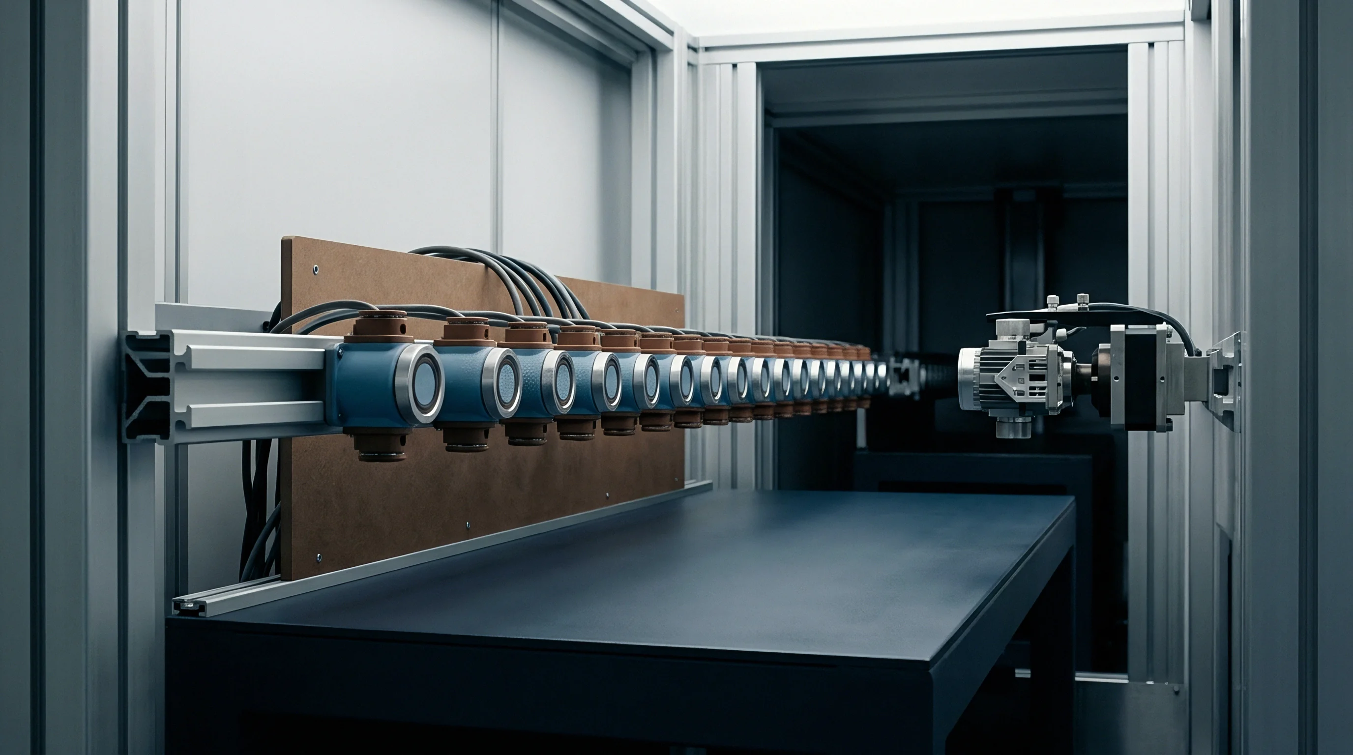
Triaxial Guarded Current Measurement at Wafer and Module Level
Sub-nanoampere leakage measurements require guarded measurement techniques to eliminate stray parasitic paths within test fixtures and cabling. Triaxial cables maintain a secondary guard conductor at the same electrical potential as the central force-sense signal line. Coaxial cables introduce unacceptable dielectric leakage and cable capacitance errors when measuring high-impedance isolation structures at high temperatures.
Wafer-level characterization uses specialized thermal chucks capable of maintaining temperature stability within 0.1°C across ranges spanning from -40°C to 250°C. Test structures feature dedicated four-terminal Kelvin contacts connected to individual piezoresistors, isolated n-wells, and substrate ground taps. High-voltage source-measure units sweep reverse-bias potentials across p-n junction interfaces while recording leakage current responses.
- Mount the un-packaged silicon MEMS die or wafer onto a temperature-controlled triaxial chuck connected to a shield enclosure.
- Connect primary source-measure units to Wheatstone bridge supply terminals, differential output nodes, and n-well bias contacts.
- Establish thermal equilibrium at the initial test temperature step, verifying zero mechanical strain via an optical laser vibrometer.
- Apply nominal bridge excitation voltage while sweeping n-well bias potentials from ground up to maximum rated supply voltage.
- Record reverse leakage currents at each bridge node using automated picoammeters configured with triaxial guard driving.
- Step environmental chamber temperature through defined thermal increments up to maximum target temperature limits.
- Extract Shockley-Read-Hall and diffusion leakage components by fitting current-voltage curves against theoretical temperature models.
Guarded triaxial measurement configurations eliminate parasitic fixture leakage down to limits below 100 femtoamperes at 200°C test temperatures.
Variable pressure chambers combine thermal cycling with controlled mechanical loading to isolate stress-induced piezoresistive shifts from junction leakage effects. Applying hydrostatic pressure inside an isothermal chamber isolates band-gap splitting parameters without inducing non-uniform thermal strain gradients across the sensor die. Differential analysis separates pure piezoresistive output changes from parasitic junction shunts.

Extracting Thermal Activation Energy of Parasitic Leakage Channels
Arrhenius plotting identifies primary leakage mechanisms across distinct operational temperature bands. Plotting the natural logarithm of measured leakage current against inverse absolute temperature yields slope values corresponding to effective activation energy. An activation energy near 1.12 electronvolts, matching the bandgap energy of silicon, confirms neutral-region diffusion leakage dominance.
Activation energies near 0.55 electronvolts point to space-charge generation mediated by mid-gap recombination centers.
Standard qualification procedures defined under IEC 60747-5 specify test conditions for semiconductor isolation interfaces. Parameter extraction dossiers must record reverse leakage current levels under maximum rated thermal and electrical stress limits. Devices exhibiting abnormal activation energies during preliminary wafer screening indicate metallic contamination or un-annealed lattice damage within the depletion region.
Per IEC 60747-5 Clause 7.3.2, parametric isolation compliance requires reverse breakdown margins to exceed 150 percent of maximum rated bridge supply voltage across the complete operating temperature range.


Guarding
Advanced micro-machining processes utilize physical and dielectric isolation techniques to eliminate p-n junction parasitic leakage pathways entirely. Bulk silicon substrates relying purely on reverse-biased junctions hit physical operational limits around 150°C to 175°C. Extending pressure transducer operation up to 250°C or 300°C demands structural isolation technologies that replace p-n junctions with solid dielectric barriers.

Dielectric Trench Isolation in Silicon on Insulator Substrates
Silicon-on-Insulator (SOI) MEMS technology provides dielectric isolation by constructing piezoresistors inside a thin single-crystal silicon device layer separated from the handle substrate by a thick Buried Oxide (BOX) layer. The buried silicon dioxide layer, typically 1.0 to 3.0 micrometers thick, exhibits wide energy bandgap properties, preventing carrier flow into the underlying silicon substrate. Buried oxide layers maintain electrical isolation resistance above 10 gigohms even at 300°C.
Lateral electrical isolation between adjacent piezoresistors on SOI wafers utilizes Deep Reactive Ion Etching (DRIE) combined with oxide refill techniques. Etching vertical trenches down to the buried oxide layer and backfilling them with thermal silicon dioxide and chemical vapor deposited polysilicon forms complete dielectric enclosures around each sensing element. Oxide trench isolation completely removes p-n junctions from the device architecture, eliminating reverse-bias leakage, space-charge generation, and parasitic PNPN latch-up risks.
| Isolation Architecture | Maximum Operating Temp (°C) | Leakage Current Density @ 200°C (nA/mm^2) | Zero-Point Thermal Drift (% FS/100°C) | Relative Die Cost Factor | Dominant High-Temp Failure Mode |
|---|---|---|---|---|---|
| Bulk Silicon P-N Junction | 150 | 15,880.00 | ± 2.85 | 1.00 | Junction Leakage Shunt |
| Diffused N-Well Guard Ring | 175 | 2,450.00 | ± 1.20 | 1.25 | Substrate Crosstalk Overflow |
| SOI with DRIE Oxide Trenches | 300 | 0.05 | ± 0.15 | 2.80 | Diaphragm Oxide Stress Drift |
| Polysilicon on SiO2 Membrane | 250 | 0.12 | ± 0.45 | 1.65 | Grain Boundary Carrier Trapping |
Active Guard Rings and Substrate Bias Routing
Where bulk silicon processes must be used due to cost constraints, active guard ring topologies mitigate leakage impacts. Highly doped n-type (n+) guard rings completely surround p-type piezoresistors. Connecting these guard rings to independent low-impedance buffer amplifiers holds the guard rings at the exact electrical potential of the enclosed piezoresistor nodes.
Equipotential guarding eliminates voltage gradients across the junction interface, reducing parasitic leakage current flow to minimal levels.
Selecting appropriate isolation architectures involves balancing raw performance requirements against manufacturing unit costs and thermal constraints. SOI processes double or triple wafer substrate acquisition costs but eliminate complex compensation circuits required for bulk junction-isolated devices.
- Silicon On Insulator Substrates eliminate substrate junction leakage channels completely, providing stable operation above 250°C.
- Deep Reactive Ion Etched Trenches establish dielectric side-walls around sensing traces, eliminating lateral parasitic current paths.
- Equipotential Active Guarding suppresses bulk junction leakage currents by maintaining zero potential difference across isolation boundaries.
- Heavy Boron Doping Configurations stabilize piezoresistive temperature coefficients at the expense of lower absolute pressure sensitivity.
High-temperature applications operating above 200°C favor dielectric trench-isolated SOI processes due to the complete elimination of parasitic p-n junction conduction mechanisms. Polysilicon-on-insulator designs offer lower wafer costs than single-crystal SOI, but grain boundary carrier trapping reduces overall piezoresistive scale factor stability under continuous pressure cycling. System designers select bulk p-n junction structures primarily for low-cost, ambient-temperature applications where operating environments remain comfortably below 125°C.