Application Method
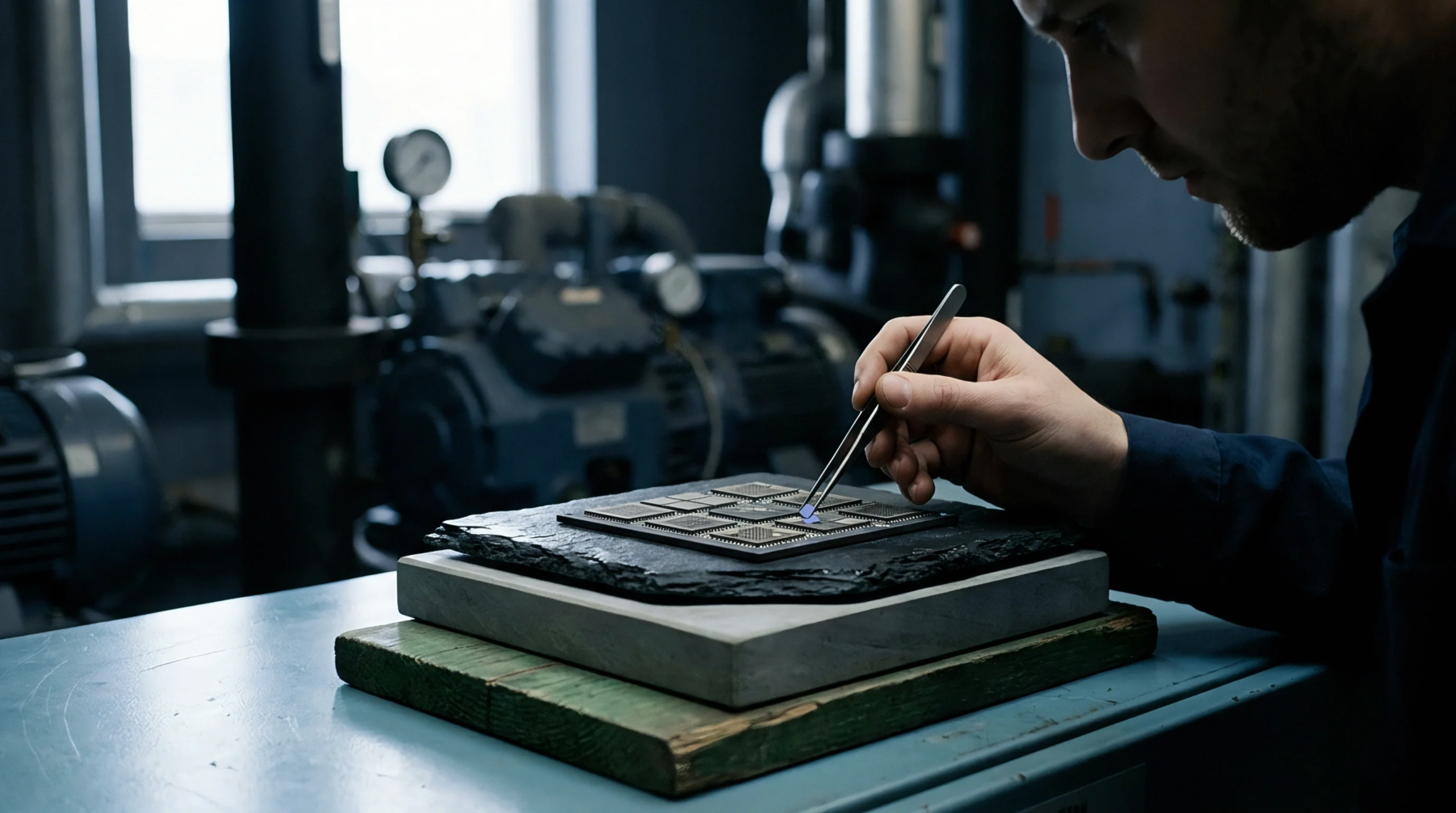
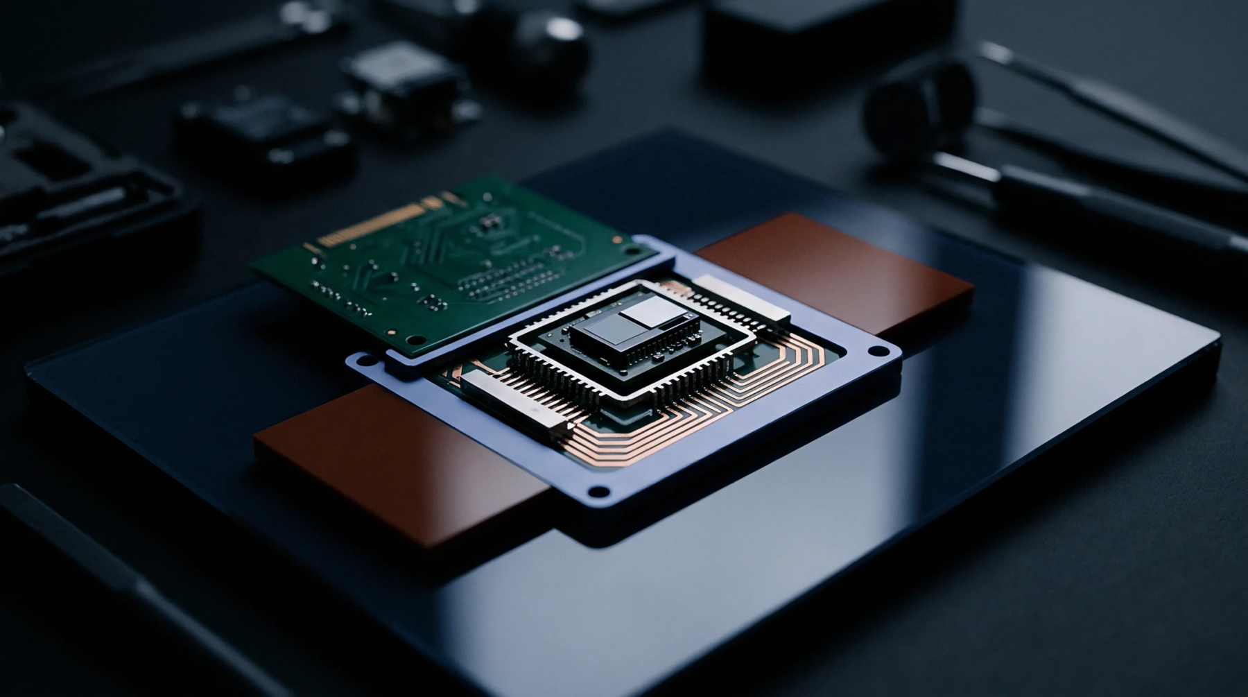
Assembly processes secure a semiconductor chip to a substrate or lead frame using adhesive or solder. In microelectronics, die attach provides the mechanical bond and the heat path between the silicon and the package. The selection of the bonding medium depends on the heat dissipation requirements and the coefficient of thermal expansion of the materials.
It is the primary interface for heat transfer out of the active device.
Process Control
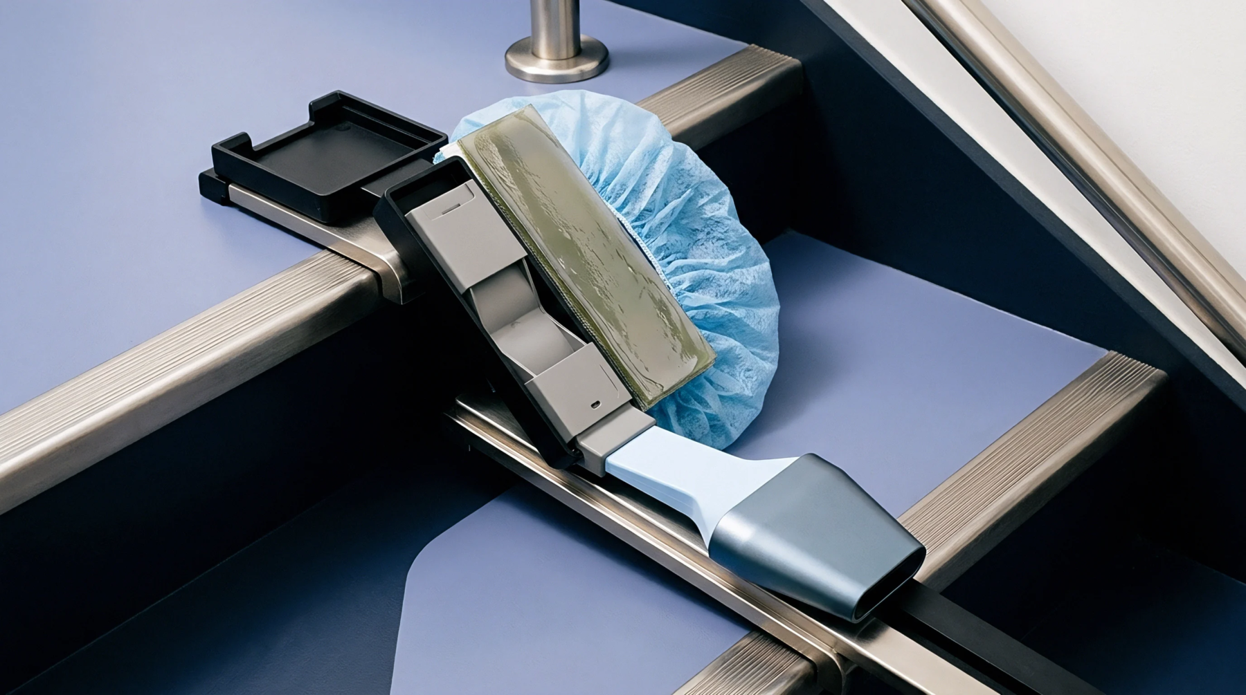
Equipment for this process includes high speed pick and place machines equipped with precise dispensing systems. During die attach, the machine applies a controlled volume of epoxy or a preform of solder to the target area. The placement force and the time of contact are critical to achieving a uniform bond line thickness.
If the bond is uneven, it creates hot spots or mechanical stress concentrations that lead to premature failure.
Reliability Stress
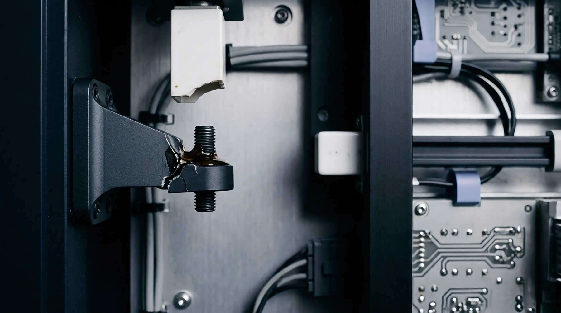
Thermal cycling tests identify weaknesses in the bond layer that could lead to delamination. Because die attach involves joining materials with different expansion rates, the interface experiences substantial shear forces when the temperature changes. Voids within the adhesive or solder layer act as starting points for cracks.
These gaps are often detected using scanning acoustic microscopy or X-ray inspection after the curing or reflow cycle. A well executed bond remains stable throughout the life of the component.
Bonding Tolerance
Specifications define the maximum allowable tilt and rotation of the chip relative to the substrate. Measuring the fillet height around the perimeter confirms that the die attach material has wetted the surfaces correctly. These metrics ensure the electrical connections made in later steps are successful.