Quantifying Micro-Mechanical Reflow Stress Variations across High-Density Multi-Layer Laminate Sensor Substrates
Unbalanced copper planes and high-modulus die attach adhesives in laminate sensor packages cause reflow-induced warpage that shifts piezoresistive zero points.


Warp
Laminate sensor packages warp during peak convection exposure because the constituent materials expand at unequal rates across the vertical build. A standard bismaleimide-triazine (BT) resin core exhibits a coefficient of thermal expansion of 15 ppm/K along the horizontal plane. Silicon dies embedded or mounted on that structure exhibit an expansion coefficient of 2.6 ppm/K. When temperatures reach the 260 °C liquidus plateau of lead-free SAC308 or SAC305 solder alloys, the mismatch imposes severe bending moments across the laminate structure.
Asymmetrical distribution of internal copper planes drives out-of-plane displacement into either a concave (crying) or convex (smiling) orientation. The resulting deflection changes the mechanical boundary condition of the sensing membrane, piezoresistive bridge, or resonant micro-beam.
Displacement tolerances across a 10 mm by 10 mm multi-layer substrate typically reach 15 µm to 40 µm at room temperature. At peak reflow temperatures, that value escalates beyond 85 µm when copper balancing across dielectric layers falls below 80 percent parity. This transient curvature exerts tensile and compressive forces on the die attach layer, which directly transmits shear loads into the active silicon bulk.
If the package cools through the solidus transition at 217 °C, the solder joints solidify around a distorted geometry. The substrate retains plastic deformation, locking residual micro-strains into the sensing elements.
IPC-7093 Class 3 assemblies penalize substrate out-of-plane distortion exceeding 50 µm across high-density land arrays by triggering automatic joint rejection during post-reflow acoustic microscopy.
Substrate thickness directly modifies the mechanical stiffness of the assembly. A thin four-layer substrate of 0.4 mm nominal thickness deflects under reflow with four times the displacement of an eight-layer 0.8 mm substrate. The thinner laminate offers lower profile height for mobile applications, yet transfers board-level assembly strain straight into the MEMS transducer cavity.
Designers selecting package formats must evaluate the mechanical trade-off between vertical envelope and offset stability.

Out-of-Plane Displacement and Plane Balancing
Dielectric layer symmetry controls the thermal moment vector. Multi-layer laminate constructions incorporate alternating layers of copper foil and pre-impregnated glass-epoxy weaves. When top routing layers demand high trace density and inner reference planes retain unbroken copper pours, the vertical neutral axis shifts away from the physical center of the substrate.
Thermal expansion produces a non-uniform strain tensor across the package z-axis. The resulting curvature causes non-planar solder paste compression during furnace entry.
Solder paste volume variations compound the substrate deflection. Outer perimeter pads on an LGA-16 or LGA-24 land pattern experience tensile lifting while center ground pads experience excess compressive squeeze-out. Solder bridging occurs under the center array, whereas perimeter joints suffer open circuits or partial wetting.
The table below lists displacement values recorded across various substrate configurations during convection reflow profiles.
| Package Format | Layer Count | Substrate Thickness (mm) | Die Thickness (µm) | Peak Displacement at 260 °C (µm) | Residual Room-Temp Warpage (µm) |
|---|---|---|---|---|---|
| LGA-12 (2.0 x 2.0 mm) | 2 | 0.20 ± 0.02 | 100 ± 5 | 18 ± 3 | 6 ± 2 |
| LGA-16 (3.0 x 3.0 mm) | 4 | 0.35 ± 0.03 | 150 ± 10 | 32 ± 4 | 12 ± 3 |
| BGA-64 (5.0 x 5.0 mm) | 6 | 0.60 ± 0.04 | 200 ± 10 | 54 ± 6 | 21 ± 4 |
| LGA-24 (4.0 x 4.0 mm) | 8 | 0.80 ± 0.05 | 250 ± 15 | 41 ± 5 | 16 ± 3 |
Solder ball and land geometry dictate the compliance of the final interconnect. Solder bump height variations alter the stand-off distance between the laminate bottom and the host printed circuit board. A shorter stand-off concentrates shear stress inside the peripheral solder joints, transferring secondary bending moments back into the laminate core upon cooling.
Factory engineers often attribute anomalous post-assembly offset shifts to ambient humidity absorption or board-level screw torque rather than addressing uncompensated trace density gradients inside the substrate itself.


Foil
Copper distribution across internal laminate routing planes acts as the primary mechanical driver of local stress gradients. High-density interconnect (HDI) substrates utilize electrodeposited copper with thicknesses ranging from 9 µm (quarter-ounce) to 18 µm (half-ounce). Traces routed with sharp 90-degree transitions create localized stress concentration zones under thermal cycling.
Differential copper area coverage between adjacent quadrants generates asymmetric lateral forces that pull the die attach interface during temperature ramps.
Blind and buried micro-vias further modify the local stiffness of the laminate matrix. Laser-drilled micro-vias filled with electroplated copper create rigid vertical columns that resist vertical thermal expansion. The surrounding resin-impregnated dielectric expands at roughly 50 ppm/K above its glass transition temperature of 170 °C. This differential rate puts the micro-via barrel in tension and shears the surrounding dielectric bond, creating localized micro-cracking and erratic mechanical support directly beneath the silicon die pad.

Via Structures and Thermomechanical Coupling
Micro-via arrays placed directly under a MEMS cavity change the acoustic and mechanical boundary conditions of the sensor. Staggered micro-vias distribute thermal stresses across a wider dielectric volume, lowering peak localized shear. Stacked micro-vias offer routing density advantages, yet behave as stiff thermal posts that transfer baseboard deflections directly to the die interface.
Solder reflow amplifies this rigidity, producing micro-cleavage along the via-to-capture-pad junction.
- Micro-via pitch clustering concentrates vertical expansion forces beneath the center of the silicon die, driving convex bending of the active transducer area.
- Unequal trace densities across orthogonal axes generate torsional moments that warp the die mounting plane out of true squareness.
- Copper thieving patterns added to empty substrate zones normalize the thermal mass and balance thermal contraction rates across the array.
- Differential pad sizing between signal lands and central ground planes produces uneven surface tension pull during solder liquidus phases.
Etching tolerances in thin core layers also introduce lateral variability. A nominal 50 µm trace width held to a ±8 µm etching tolerance produces a 16 percent variation in local copper cross-section. This variation shifts the local thermal expansion profile across individual substrate manufacturing panels.
High-volume sensor procurement schedules face batch-to-batch zero-point drift variations traceable to these etching variations.
Thieving densities matched to routing trace density within a five percent margin prevent rotational substrate distortion during convection cooling.
The choice of core dielectric materials dictates the base rate of thermal expansion. Standard FR-4 glass-epoxy systems exhibit high z-axis expansion rates exceeding 60 ppm/K. Specialized low-loss hydrocarbons or polyimide-based laminates restrict out-of-plane expansion to 25 ppm/K to 35 ppm/K. Sourcing teams paying a unit price premium of $0.08 to $0.15 for high-Tg BT-epoxy substrates recover that expense through reduced calibration trim rejects on the assembly line.
Solder joint reliability drops when trace layout choices ignore the symmetry of internal planes.


Piezoresistance
Silicon sensing elements alter their electrical resistivity when mechanical strains propagate through the crystal lattice. In monocrystalline silicon, the piezoresistive coefficients along the and crystallographic orientations dictate the magnitude of the signal shift. Reflow-induced stresses reaching 40 MPa to 120 MPa induce fractional resistance shifts on internal resistors.
For uncompensated bridge configurations, this stress level produces output zero-point offsets exceeding 15 millivolts on a 3.3 V supply rail.
Analog front-end circuits amplify these offset errors directly into the measurement signal chain. In pressure sensors and tri-axial accelerometers, reflow strain manifests as a permanent sensitivity shift alongside an offset error. When packaging houses transition an existing die from a ceramic carrier to a molded multi-layer laminate LGA, the baseline factory calibration becomes invalid.
The high compliance of organic substrates creates an expanded hysteresis envelope across temperature operating ranges from -40 °C to 125 °C.
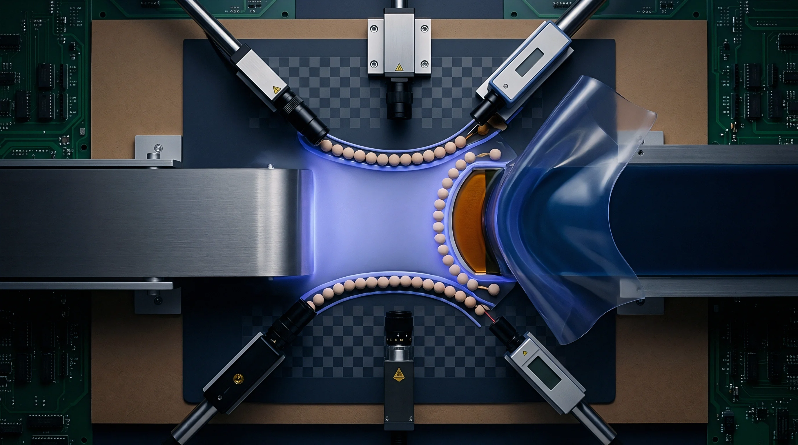
Mechanical Strain and Crystallographic Orientation
Stress sensitivity varies substantially across p-type and n-type doped silicon regions. P-type diffused resistors oriented along the longitudinal crystal axis exhibit high sensitivity to normal stresses, while transverse stresses contribute secondary cross-axis errors. Solder reflow creates multi-axial stress fields containing both normal and in-plane shear components.
Die layout geometry must balance resistor placements symmetrically relative to the package neutral axis.
| Doping Type | Orientation Axis | Piezoresistive Coeff. (10⁻¹¹ Pa⁻¹) | Induced Stress (MPa) | Fractional Resistance Shift (%) | Offset Shift (mV / V) |
|---|---|---|---|---|---|
| p-type (Boron) | Longitudinal | +71.8 | 65 ± 10 | 0.47 ± 0.07 | 2.35 ± 0.35 |
| p-type (Boron) | Transverse | -66.3 | 45 ± 8 | -0.30 ± 0.05 | -1.50 ± 0.25 |
| n-type (Phosphorus) | Longitudinal | -102.2 | 65 ± 10 | -0.66 ± 0.10 | -3.30 ± 0.50 |
| n-type (Phosphorus) | Transverse | +53.4 | 45 ± 8 | 0.24 ± 0.04 | 1.20 ± 0.20 |
| Calculated for uniform silicon membrane dopant concentrations of 10¹⁸ cm⁻³ at 25 °C under biaxial reflow loading. | |||||
Die attach adhesives serve as the primary mechanical buffer between the laminate substrate and the active silicon element. High-modulus epoxy adhesives transmit roughly 85 percent of substrate reflow strain directly into the die. Low-modulus silicone adhesives, with a Young’s modulus below 5 MPa, absorb thermal shear strain and attenuate stress transfer to less than 15 percent.
Silicone die attach materials introduce risks of outgassing and require extended cure profiles that increase cleanroom cycle times.
A soft silicone die attach layer with Young’s modulus below 3 MPa limits reflow-induced piezoresistive offset shift to less than 0.5 millivolts per volt of excitation.
Mechanical stress also alters the bandgap of integrated reference diodes within on-die voltage regulators. Bandgap reference circuits undergo thermal hysteresis when package stress changes the junction potential of bipolar transistors. A one-millivolt shift in the on-chip reference voltage translates to a 0.03 percent full-scale measurement error in a 16-bit analog-to-digital converter.
Firmware engineers debugging sensor inaccuracies frequently spend weeks tuning digital filters before recognizing that the source of the drift resides in the packaging physics.
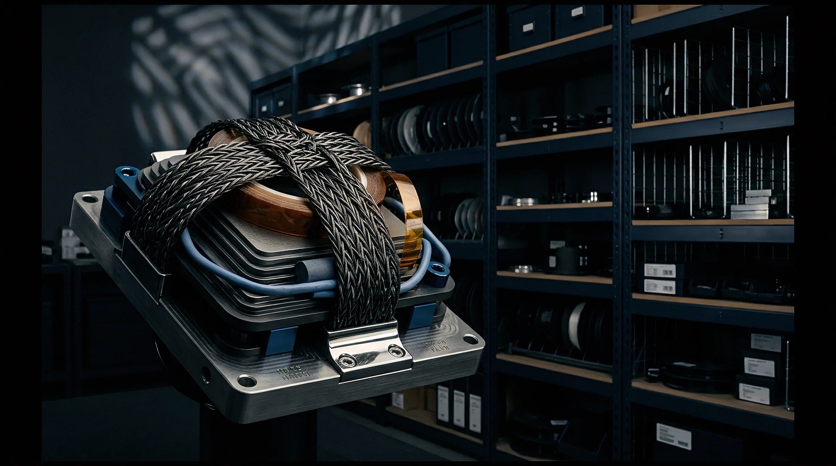
Digital Interface Bus Timing and Stress Recovery
Modern sensor variants integrate digital interface logic on the same die or as a co-packaged ASIC. These parts communicate over I2C, SPI, or I3C buses. Substrate warpage and mechanical stress can alter the internal clock oscillator frequency by several percent through piezoresistive effects on silicon timing cores.
A nominal 400 kHz Fast-Mode I2C clock frequency shifting by 4 percent alters bus timing margins and increases communication frame errors when long PCB trace capacitances approach the 400 pF bus limit.
The procurement decision between an analog raw sensor and an integrated digital package rests on calibration complexity. An analog sensor component carries a lower bill of materials unit price ($0.85 versus $1.65 for a calibrated digital counterpart at 10,000 unit volumes). The raw analog component demands factory multi-point thermal calibration and laser trimming on the host board to zero out reflow-induced piezoresistive offsets.
The calibrated digital variant incorporates internal lookup tables and polynomial compensation routines running inside the package ASIC, absorbing the reflow stress shift before outputting calibrated engineering units over SPI or I2C.
The total cost of implementation shifts rapidly toward digital interface variants once factory programming fixture maintenance, test chamber cycle times, and yield fallout from uncompensated analog drift enter the financial ledger.
What remains unquantified across high-volume production lines is whether long-term room-temperature viscoelastic stress relaxation in organic die attach adhesives gradually invalidates digital polynomial coefficients programmed immediately after reflow cooling.
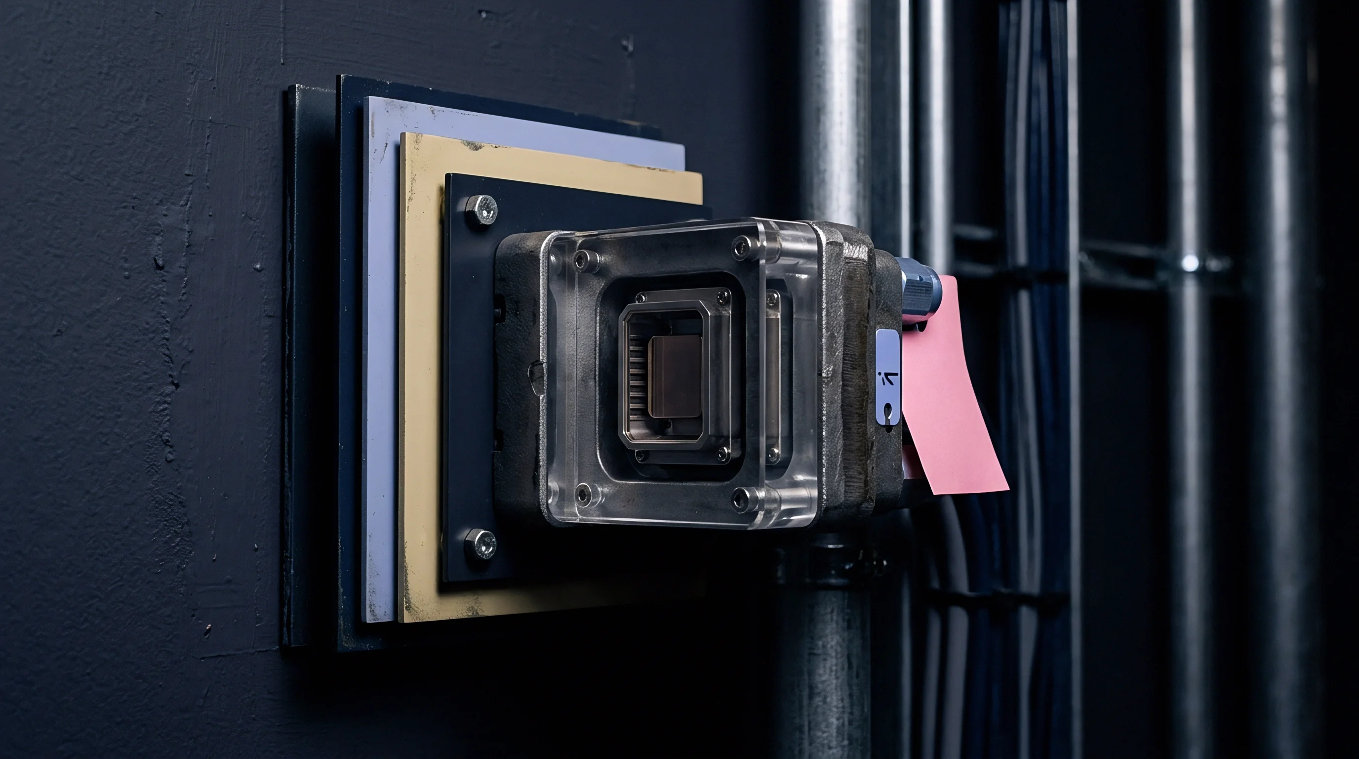

Hysteresis
Thermal cycling induces permanent zero-point drift because organic laminates undergo non-reversible viscoelastic deformation under repeated temperature excursions. A standard reflow thermal excursion heats the assembly past the glass transition temperature of the epoxy resin. Polymer chains re-orient into lower-energy conformational states, altering the baseline mechanical stress state of the cured substrate.
Upon cooling, the laminate does not return to its exact pre-reflow dimensional state. This residual mechanical hysteresis creates a static offset in sensor readings that persists indefinitely unless compensated by field recalibration.
Moisture absorption accelerates viscoelastic settling in high-density laminate structures. Hydrophobic epoxy systems absorb up to 0.5 percent atmospheric moisture by weight when stored outside moisture barrier bags. During reflow heating, the rapid vaporization of trapped water molecules creates micro-cavities and hydro-mechanical pressure within the dielectric weave.
This internal swelling weakens resin-to-fiber adhesion, permanently reducing substrate flexural modulus and shifting the mechanical zero point of mounted sensor dies.

Viscoelastic Settling and Offset Drift
Stress relaxation kinetics follow a logarithmic decay profile over extended operating periods. A sensor package fresh from the reflow furnace exhibits rapid zero-point drift during the initial 72 hours of ambient storage. The rate of relaxation slows over subsequent weeks as polymer chains reach mechanical equilibrium.
Performing end-of-line electrical calibration too soon after reflow locks premature baseline values into non-volatile memory, guaranteeing field measurement errors as the substrate continues its relaxation cycle.
- Incoming package moisture inspection verifies barrier bag integrity and desiccator humidity indicator cards prior to high-speed tape-and-reel feeding.
- Reflow peak dwell time control limits component exposure above the 217 °C liquidus line to between 60 and 90 seconds, restricting resin plasticization.
- Controlled post-reflow stabilization bake holds assembled circuit boards at 85 °C for 24 hours to accelerate initial viscoelastic stress relief before test execution.
- Multi-temperature offset capture samples sensor zero points across three operational temperature tiers to populate host firmware compensation tables.
- Acoustic scanning verification screens production samples for internal delamination between laminate dielectric layers and copper planes.
Package form factor selection strongly influences hysteresis magnitude. Molded Leadless Packages (MLP) and Quad Flat No-Lead (QFN) devices feature exposed metallic thermal pads that solder directly to the motherboard. This large solder interface anchors the package rigidly to the host PCB, transmitting every board-level thermal expansion directly to the sensor die.
Land Grid Array (LGA) formats use distributed micro-pads that provide greater mechanical compliance, isolating the sensing element from host board expansion moments.
| Package Architecture | Interconnect Type | Board Area (mm²) | Reflow Hysteresis (ppm FS) | Firmware Bring-Up (Weeks) | Unit Cost at 50k Volume |
|---|---|---|---|---|---|
| Bare SMD LGA | Direct Land Solder | 9.0 | 450 ± 60 | 4 | $1.45 |
| Overmolded QFN | Exposed Pad + Leads | 16.0 | 850 ± 110 | 3 | $1.15 |
| Embedded Die Substrate | Micro-via Direct | 6.2 | 1200 ± 180 | 6 | $2.80 |
| Pre-Calibrated Module | Header / Castellated | 64.0 | 80 ± 15 | 1 | $4.60 |
| Housed Probe Assembly | Cabled M8 Connector | 350.0 | 15 ± 5 | 1 | $18.50 |
Procurement teams balancing unit cost against system performance must weigh the hidden costs of firmware engineering and factory calibration fixtures. Sourcing an uncalibrated QFN device at $1.15 cuts upfront bill of materials spending. Developing custom firmware compensation routines to eliminate its 850 ppm reflow hysteresis consumes weeks of software engineering time and extends factory testing cycles by several seconds per board.
Failure to account for post-assembly stress relaxation results in systematic field measurement drift and premature warranty liability across precision industrial instruments.


Qualification
Procurement contracts for high-density laminate sensor components must specify strict mechanical stability metrics alongside standard electrical parametrics. Standard distributor line items guarantee digital communication functionality, pinout geometry, and gross parametric operating envelopes. They rarely provide guarantees regarding maximum package warpage during reflow or maximum permissible post-soldering offset drift.
Sourcing managers must write precise acceptance thresholds directly into custom master service agreements and technical delivery specifications.
Incoming inspection protocols for high-density substrates require dedicated thermomechanical characterization. Optical shadow moiré interferometry serves as the primary verification tool for measuring real-time package warpage across dynamic reflow thermal profiles. Contract manufacturing facilities lacking shadow moiré capabilities cannot verify whether incoming substrate lots meet IPC-9641 warpage specifications, exposing projects to sudden assembly yield drops.

Contractual Clauses and Acceptance Sampling
Incoming material lots require destructive and non-destructive mechanical screening. Cross-sectional micro-sectioning verifies internal copper plane symmetry, dielectric layer thickness consistency, and micro-via barrel plating integrity. Non-destructive acoustic micro-imaging detects internal voids within die attach epoxy layers before components reach surface-mount placement machines.
Substrates exhibiting uneven copper etching or resin voids must face immediate batch rejection before board assembly.
- Shadow moiré warpage profiles demonstrating maximum z-axis deflection below 35 µm across the entire 20 °C to 260 °C thermal trajectory.
- Copper distribution balance certificates verifying that internal metal volume fractions between opposing laminate layers remain within a 5 percent tolerance band.
- Post-reflow zero-offset drift limits bounding sensor output shifts to less than 0.2 percent of full-scale span following a standard JEDEC J-STD-020 lead-free reflow cycle.
- Die attach modulus and glass transition reports documenting that adhesive mechanical properties match qualified design parameters within ±10 percent.
Automotive qualification under AEC-Q100 Grade 1 mandates rigorous temperature cycling from -40 °C to 125 °C for 1,000 cycles without functional or parametric failure. Laminate-packaged sensors subjected to this regimen frequently experience cumulative piezoresistive zero-point drift due to progressive solder fatigue and dielectric micro-cracking. Sourcing components certified to AEC-Q100 requires verifying that the qualification report explicitly monitors analog sensor zero-point stability throughout the thermal test duration, rather than merely verifying digital I2C bus responsiveness at end-of-test checkpoints.
Lead-time volatility in specialty substrate materials presents a commercial risk. High-Tg BT-epoxy laminates and low-modulus silicone die attach adhesives carry raw material lead times extending from 16 to 26 weeks. Sourcing strategies that rely on spot-market substitutions of alternative laminate core materials without prior thermomechanical requalification inevitably encounter severe post-assembly offset drift during production runs.
AEC-Q100 Grade 1 qualification requires monitoring analog output zero-point stability across all 1,000 thermal cycles to ensure that cumulative laminate strain does not exceed design tolerances.
Engineering change notices (ECN) issued by packaging sub-contractors frequently alter internal leadframe alloys, substrate core suppliers, or mold compound formulations without modifying external package dimensions. These silent revisions change the thermomechanical stress tensor of the package entirely. Sourcing agreements must mandate formal notification and client sign-off for any internal bill of materials alteration, ensuring that the mechanical interface between the sensor die and the host circuit board remains stable throughout the complete product manufacturing lifecycle.
JEDEC J-STD-020 Table 5-1 establishes the maximum allowable component package peak temperature and floor life conditions, governing whether a lot passes incoming dock audits without re-baking.