
Interferometric Fiber Optic Gyroscope Scale Factor Mechanics
Optical scale factor in closed-loop IFOGs locks rotation velocity to digital ramp resets bounded by coil geometry, source wavelength, and 2π reset accuracy.
Optical scale factor in closed-loop IFOGs locks rotation velocity to digital ramp resets bounded by coil geometry, source wavelength, and 2π reset accuracy.

Silicon on insulator trench isolation eliminates lateral junction leakage above two hundred degrees by replacing reverse-biased junctions with dielectric barriers.
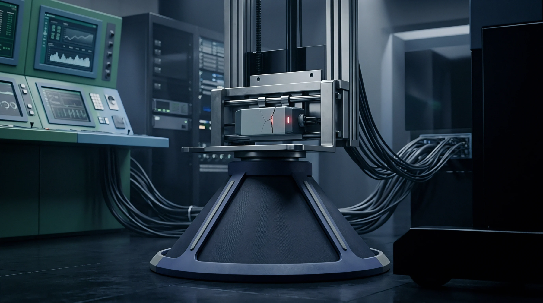
Shear stress lifts valence band degeneracy in p-type silicon, causing shear piezoresistive coefficients to decay and compress transducer gain under heavy load.

Heavy boron doping flattens piezoresistive gauge factor thermal drift but shifts baseline bridge resistance through temperature-dependent carrier mobility changes.

Thermal cycling degrades degenerate p-type silicon hole mobility via defect migration and band splitting, driving non-linear piezoresistive bridge drift.

Constant current drive cancels piezoresistive span drift by exploiting positive bridge resistance growth to offset the negative temperature coefficient of sensitivity.

Boron doping above 5.0 × 10^19 cm^-3 stabilizes thermal span drift under current excitation while dropping silicon piezoresistive gauge factor from 120 to 38.

Dynamic clock drift generates phase uncertainty in asynchronous decimation by varying fractional delay in polyphase FIR structures during downsampling.

Synchronize converter apertures to mains noise by setting sample counts to exact integer multiples of the power line period using precision master clocks.

Select converter sample rates whose decimation zeros align with nominal mains frequencies, using crystal timing to prevent drift-induced rejection loss.

Polyphase decimation stage group delay sums directly across multirate boundaries, stripping phase margin from closed-loop motion regulators at crossover.

Set moving average filter length N to an integer multiple of decimation factor M to align spectral nulls with alias bands and preserve channel group delay.
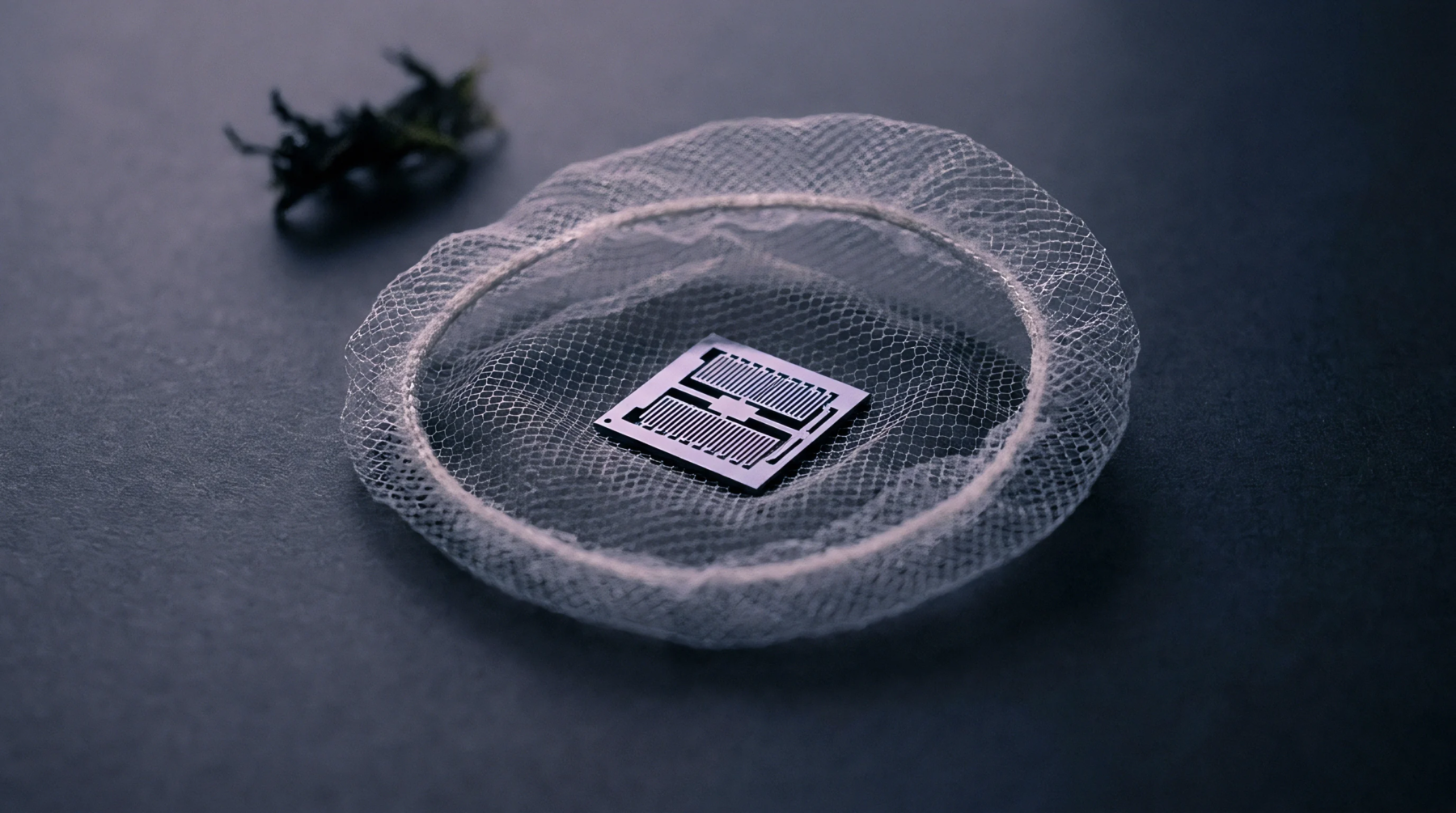
Decimated moving average filters trade stopband attenuation for low compute density by combining unweighted integration with downsampling.

Coaxial current viewing resistor skin effect attenuates high-frequency pulse harmonics, causing peak current underestimation and edge rounding in nanosecond diode drivers.

Minimizing total loop inductance below five nanohenries requires wide planar busbars, Kelvin gate drive connections, and low-inductance ceramic capacitors.
Dynamic carrier accumulation and recombination rates cause optical pulse lag, demanding DC pre-bias and active reverse charge shunts for picosecond timing.

Suppress ambient ghosting by combining narrow-band optical filtering, microsecond overdriven stroboscopic lighting, and sensors with sub-90 dB parasitic light sensitivity.

Matching strobe pulses to rolling shutter quiet windows demands subtracting line clock skews parasitic leakage delays and driver rise jitter.

Sub-microsecond LED driver jitter induces rolling shutter exposure banding; controlling it demands low-inductance loop layout and GaN gate drive topologies.

Optimal CMOS rolling shutter strobe overlap duration equals exposure time minus frame readout time, timed precisely during full-frame row integration.

Global strobe firing requires setting exposure duration beyond frame readout sweep time to form an open timing window across all sensor lines.
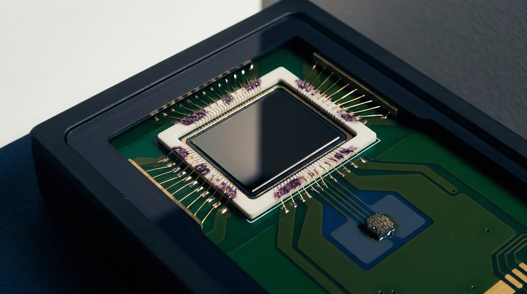
Equalize dual-sourced sensor phase delays and noise variances inside firmware signal chains to maintain control loop stability across alternate suppliers.
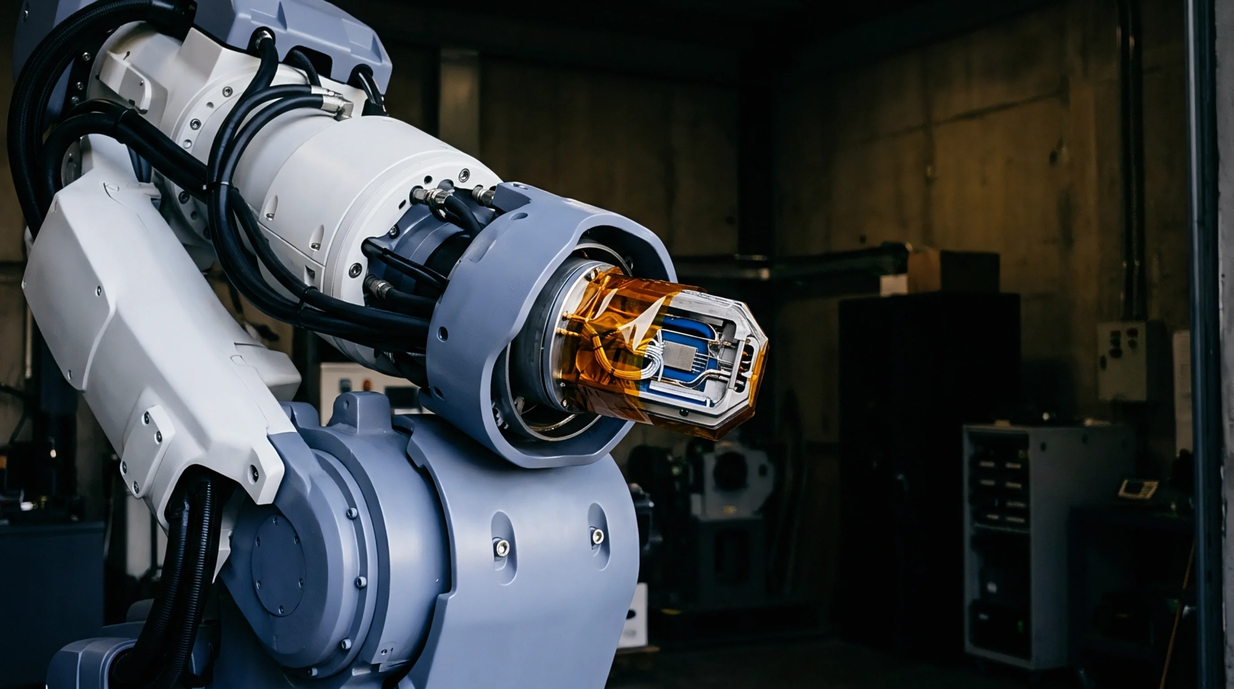
Rolling shutter LED strobe sync requires setting exposure time longer than frame scan time to create an all-row overlap window for flash pulse firing.

Secondary substrate oxygen precipitates pin dislocation lines during thermal cycles, driving long-term transducer hysteresis shifts manageable via FTIR lot screening
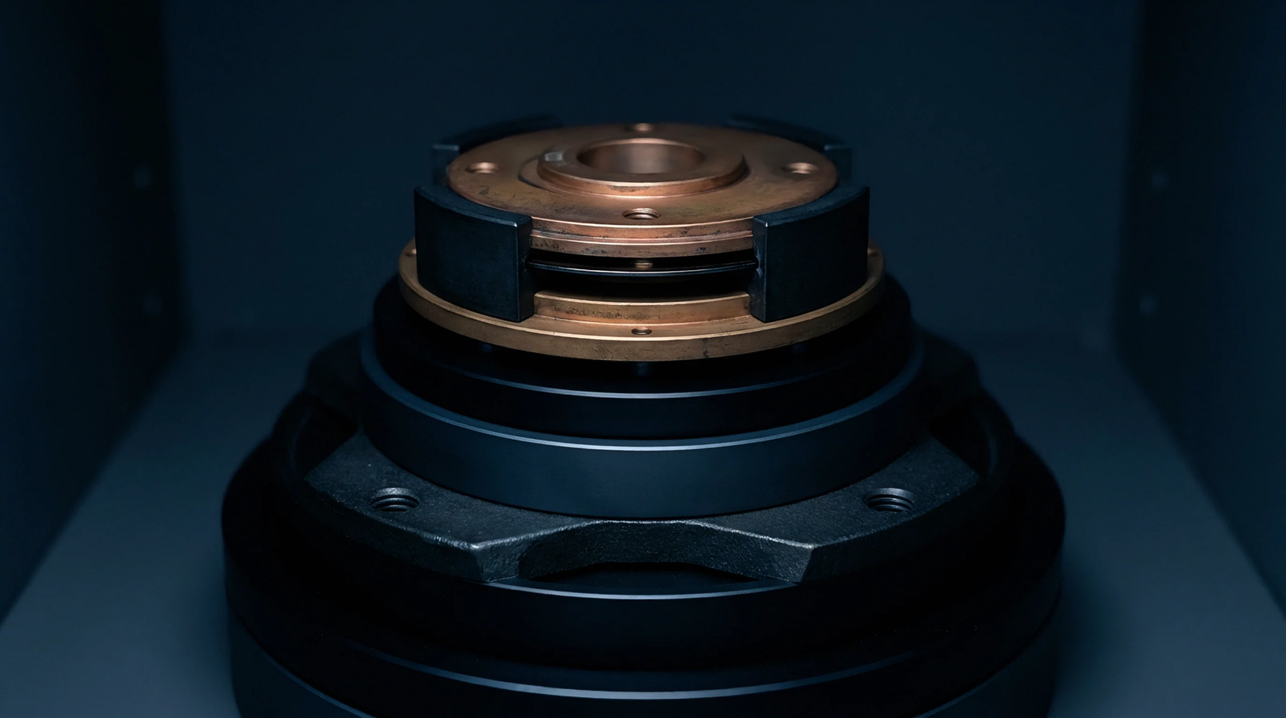
Dual foundry dynamic range calibration pairs raw bridge offset trimming with active gain scaling to preserve signal chain effective resolution across wafer lots.

Film stress variations in secondary MEMS foundries cause severe out-of-plane beam deflection, driving high post-package offset drift and severe yield losses.

Packaging-induced thermo-mechanical stress creates zero-point offset hysteresis in micro-machined sensors, requiring matched mold compound CTE calibration.
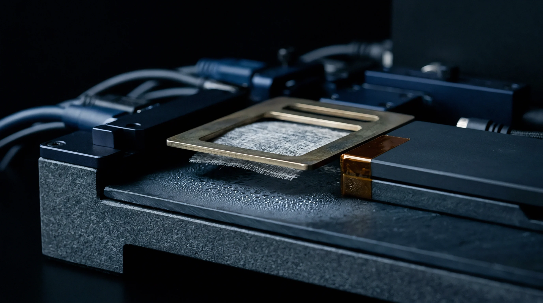
Decoupling polymer mechanical creep from ASIC bias shifts isolates baseline zero drift in uncompensated piezoresistive pressure transducers.

Modeling localized dislocation kinetics prevents slip line generation by keeping transient thermoelastic shear stresses strictly below moving critical thresholds.

Resolved shear stress exceeding critical values during thermal ramp-up triggers rapid dislocation multiplication requiring multi-wavelength pyrometry feedback.
Expertise is a utility, not a secret. sentiention™ publishes its working knowledge as open reference: intelligence layer covering the materials it sources, the markets it enters, and the reference that serves both.