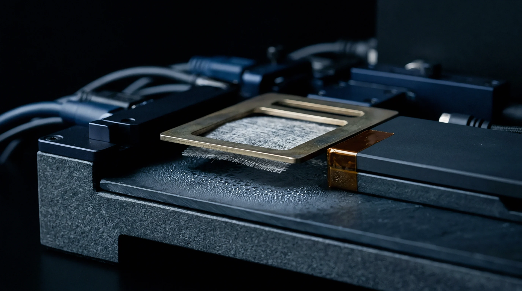
Encapsulation Technique
Semiconductor packaging relies on a protective structural housing to shield delicate silicon dies and bond wires from environmental hazards. Through the process of leadframe molding, thermosetting epoxy compounds are injected around the leadframe assembly to form a rigid, hermetically sealed package. This step secures the external pins and provides mechanical support for the enclosed microelectronics.
The cured polymer ensures thermal dissipation and electrical isolation during active operation.
Process Parameter
Control of mold temperature and injection pressure prevents damage to the fragile gold or copper wire bonds. Optimizing the transfer speed during leadframe molding ensures that the liquified epoxy fills all cavities before curing begins. Precise clamping force prevents flash, which is the unwanted escape of resin along the parting line.
Defect Mechanism
Inadequate venting or uneven resin flow can trap air, resulting in internal voids or surface pitting. If the epoxy shrinks excessively during cooling, it induces residual stresses that lead to package warping or delamination. These failures jeopardize the moisture resistance of the packaging.
Quality Assurance
Post-mold curing steps finalize the chemical cross-linking of the polymer matrix to maximize mechanical strength. Non-destructive acoustic microscopy scans the package to check for internal separation. This verification step confirms the integrity of the molded interface.