Electrical Current Rise Time Optimization in High Power Pulsed Driver Circuits
Minimizing total loop inductance below five nanohenries requires wide planar busbars, Kelvin gate drive connections, and low-inductance ceramic capacitors.


Loop

Pulsed Current Switching Dynamics
Fast energy transfer in high di/dt switching topologies depends on minimizing trace parasitic inductance. When a high-power pulsed driver discharges stored electrical energy into a low-impedance load, the rate of current rise is governed by total loop inductance according to the differential voltage relationship V equals L times di over dt. In laser diode drivers, plasma pinch circuits, pulsed electric field generators, and radar transmitters, achieving current rise times under ten nanoseconds demands loop inductances below ten nanohenries.
High peak current levels reaching hundreds or thousands of amperes exacerbate voltage transients across these parasitic inductive elements. The physical layout of the current path forms an inductive loop that stores magnetic energy during the pulse transition. Minimizing the enclosed area of this conductive path directly reduces magnetic flux coupling and loop inductance.
System designers must model the driver layout as a distributed parameter network rather than a lumped-element circuit when commutation speeds enter the sub-nanosecond domain. Parasitic loop inductance creates a voltage back-EMF that opposes current build-up during initial switch conduction. The amplitude of this back-EMF often approaches total supply voltage, reducing effective voltage applied across the load and slowing current rise time.
To counter this effect, driver design minimizes physical conductor lengths, maximizes conductor widths, and enforces close proximity between the forward current trace and the return ground path.

Planar Strip Geometry and Loop Area Reduction
Conductive traces arranged in stacked, counter-propagating configurations limit electromagnetic field expansion. Placing the forward current trace directly above the return conductor on adjacent printed circuit board layers separated by a thin dielectric allows opposing magnetic fields generated by equal and opposite currents to cancel in the surrounding space. This field cancellation significantly decreases net loop inductance compared to side-by-side trace routing.
The characteristic impedance of such planar striplines or microstrips is controlled by dielectric thickness, conductor width, and material dielectric constant.
| Layout Geometry | Layer Separation (mm) | Conductor Width (mm) | Inductance Per Unit Length (nH/cm) | Relative Rise Time Impact |
|---|---|---|---|---|
| Coplanar Traces (Side-by-Side) | 1.50 | 2.0 | 4.5 to 6.2 | Severe Degradation |
| Microstrip Over Ground Plane | 0.20 | 5.0 | 0.8 to 1.4 | Moderate Attenuation |
| Stripline (Center Layer) | 0.15 | 8.0 | 0.3 to 0.6 | Minimal Impact |
| Parallel Planar Busbars | 0.08 | 25.0 | 0.05 to 0.12 | Optimal Current Rise |
Dielectric selection controls capacitance. Decreasing dielectric thickness between stacked conductors lowers loop inductance but increases parasitic loop capacitance. The resulting LC circuit exhibits a characteristic natural frequency that sets the absolute physical ceiling for driver rise time and pulse bandwidth.
When loop inductance remains unoptimized, severe voltage overshoot occurs across the solid-state switch during turn-off, exceeding device breakdown voltage ratings and forcing catastrophic semiconductor failure.

Inductance

Loop Inductance Decomposition and Voltage Drop Mechanics
Total circuit magnetic energy storage governs the instantaneous voltage drop across high-power driver terminals. Parasitic inductance in a high-power driver originates from three distinct regions: the energy storage capacitor bank equivalent series inductance, the semiconductor package lead inductance, and the interconnect routing loop. Each contributor adds in series to impede rapid current transitions.
In a driver operating at one kilovolt with a target rise time of five nanoseconds to reach five hundred amperes, the required di/dt rate is one hundred amperes per nanosecond. Under these conditions, every single nanohenry of parasitic inductance absorbs one hundred volts of the available driving potential.
A planar busbar assembly with an internal dielectric gap of eighty micrometers yields a parasitic loop inductance below zero point one nanohenries per centimeter under a two-hundred-ampere pulse discharge.
At high di/dt rates, current distribution within copper conductors becomes non-uniform, crowding toward the outer perimeter or facing surfaces of opposing conductors. The skin depth of copper at high frequencies restricts the effective cross-sectional area, increasing high-frequency AC resistance and altering loop inductance dynamics. Multi-layer copper laminations with thin insulation layers mitigate skin effect constraints while maximizing surface area for balanced magnetic flux distribution.

Coaxial and Low-Inductance Busbar Architecture
Parallel conductive plates separated by thin dielectric layers produce balanced magnetic field cancellation. Modern pulsed driver assemblies replace conventional wire interconnections and standard printed circuit board traces with laminated low-inductance busbar structures. These busbars integrate positive and negative voltage rails into a tightly coupled sandwich structure.
The total loop inductance of a laminated busbar is proportional to insulation layer thickness and inversely proportional to busbar width. Utilizing polyimide or thin ceramic dielectrics allows insulation distances below one hundred micrometers without compromising dielectric breakdown safety margins.
- Capacitor packaging inductance introduces parasitic voltage drops across terminal leads during sudden discharge cycles.
- Semiconductor bond wire loops restrict the maximum achievable current ramp rate inside traditional transistor modules.
- Uncompensated return paths generate stray magnetic fields that inductively couple noise into sensitive gate drive circuitry.
- Dielectric breakdown degradation occurs when localized high voltage spikes exceed insulation field strength ratings.
Coaxial conductor arrangements represent an effective layout geometry for high-power pulse delivery. In a coaxial structure, the inner conductor carries discharge current to the load while the outer tubular shield serves as the current return path. Because the magnetic field outside an ideal coaxial geometry is zero, mutual flux linkage with surrounding components is eliminated.
Coaxial structures provide predictable, low-inductance characteristics over multi-gigahertz bandwidths, making them well suited for connecting pulse generator outputs directly to low-impedance loads such as laser diode arrays or plasma discharge gaps. The primary constraint remains spatial density, as coaxial connections require larger volume footprints than planar flexible circuits.
What remains unresolved in extreme high-density designs is the quantitative trade-off between spatial packaging limitations and mutual inductive cross-coupling when multiple ultra-fast driver channels are fired simultaneously in close physical proximity.
Switch

Which Gate Driver Circuit Maximizes Commutation Speed?
Push-pull stage topologies utilizing low internal gate resistance isolated ICs deliver tens of amperes within single-digit nanoseconds. Semiconductor device turn-on dynamics establish the fundamental limit for driver current acceleration. Silicon-based MOSFETs and IGBTs are constrained by internal gate resistance, junction capacitance, and package bond wire inductance.
Gallium Nitride High Electron Mobility Transistors and Silicon Carbide MOSFETs offer significantly lower input capacitances and faster channel transition speeds, enabling current rise times under two nanoseconds.
Standard IEC 60747-8 mandates that power semiconductor switching speeds be measured using non-inductive coaxial current shunts under double-pulse test setups to isolate package parasitic effects.
Gallium Nitride devices possess zero reverse recovery charge, eliminating the substantial current tail and associated power dissipation observed during commutation in conventional silicon body diodes. To exploit the ultra-fast switching capabilities of wide-bandgap semiconductors, the gate drive circuit must deliver peak gate currents of ten amperes or higher with propagation delays under fifteen nanoseconds. Gate loop inductance must be minimized by placing gate driver ICs directly adjacent to the power transistor terminals.

Semiconductor Commutation Dynamics and Kelvin Connections
Separating the high-current power return from the control gate loop prevents common source impedance feedback. In traditional three-terminal power packages, the source or emitter terminal carries both the high di/dt power current and the gate drive charging current. The parasitic inductance of this shared lead creates an opposing voltage drop during turn-on that subtracts directly from the applied gate-to-source drive voltage.
This degenerative feedback slows down channel turn-on, increases switching losses, and degrades output current rise time.
| Semiconductor Material | Device Architecture | Breakdown Voltage (V) | Typical Output Rise Time (ns) | Max Peak Current (A) |
|---|---|---|---|---|
| Silicon (Si) | Avalanche MOSFET | 500 to 1000 | 2.5 to 5.0 | 100 |
| Silicon Carbide (SiC) | Planar MOSFET | 1200 to 1700 | 5.0 to 12.0 | 400 |
| Gallium Nitride (GaN) | Enhancement-Mode HEMT | 100 to 650 | 0.5 to 1.8 | 250 |
| Gallium Arsenide (GaAs) | Photoconductive Switch | 1000 to 10000 | 0.1 to 0.5 | 1000 |
Kelvin source connections eliminate feedback. By establishing a dedicated fourth terminal directly on the semiconductor die for gate loop return, the power current return path is isolated from the gate driving circuit. This architectural separation ensures that high di/dt rates in the power loop do not induce parasitic voltages in the gate circuit, enabling uninterrupted, maximum-speed device channel charging.
Power transistor vendors frequently cite intrinsic die switching capability while omitting the realistic limits imposed by user-level printed circuit board layout parasitics and gate driver internal source resistance during actual customer integration.

Damping
Snubber Topologies and Energy Loss Trade-Offs
Energy dissipation networks mitigate high-frequency parasitic ringing without excessively suppressing signal edges. In high-power drivers with sub-five-nanosecond current rise times, circuit stray inductance interacts with semiconductor junction capacitance to form an underdamped high-frequency resonant tank circuit. This resonance induces large voltage overshoots and sustained high-frequency ringing following the initial pulse edge.
Unchecked voltage oscillations subject power switches to excessive voltage stress, generate intense electromagnetic interference, and distort the load current pulse profile.
Resistive-capacitive snubber networks placed across power switches damp these oscillations by absorbing high-frequency transient energy. The snubber capacitor must be selected to be larger than the semiconductor output capacitance, while the snubber resistor matches the characteristic impedance of the parasitic resonant circuit. However, conventional RC snubbers dissipate energy during both turn-on and turn-off transitions, introducing significant power losses that scale linearly with operating pulse repetition frequency.
Resonant snubbers or energy-recovery active clamps offer alternative solutions by returning excess parasitic energy back to the primary supply rail.

Active Damping and Gate Resistor Tuning
Modulating series gate impedance during turn-on controls channel switching speed dynamically. Simple fixed gate resistors force a compromise between turn-on rise time and transient voltage overshoot. A lower gate resistance accelerates rise time but increases di/dt, heightening voltage spikes caused by parasitic inductance.
Conversely, increasing gate resistance suppresses overshoot at the cost of significantly longer rise times and higher thermal dissipation in the switch die.
- Connect an active high-bandwidth coaxial current shunt in series with the low-side return terminal of the pulsed driver load.
- Attach a double-shielded fifty-ohm coaxial transmission line from the shunt output to a high-sample-rate digital oscilloscope terminated in fifty ohms.
- Set the initial adjustable series gate resistor to its maximum design value to ensure overdamped circuit performance during initial pulse testing.
- Gradually reduce the turn-on series gate resistance in small increments while observing the pulse current rise time and overshoot amplitude on the oscilloscope.
- Stop decreasing resistance when the peak voltage overshoot across the switch reaches eighty percent of the maximum semiconductor breakdown voltage rating.
Adjusting the snubber network time constant to equal the resonant period of the primary parasitic loop eliminates unwanted oscillations without needlessly degrading edge transition rates.

Metric

Coaxial Shunts and Viewing Resistor Transduction
Accurate current waveform capture at sub-nanosecond scale demands transducers with low insertion impedance and high signal bandwidth. Standard inductive current transformers and low-cost Hall-effect sensors suffer from bandwidth limitations and core saturation when subjected to high-amplitude, high di/dt pulsed currents. Coaxial current viewing resistors, also known as Park shunts, provide linear transduction performance from direct current up to multi-gigahertz bandwidths.
Maintain strict physical symmetry in coaxial currentViewing resistor mounting configurations to avoid introducing artificial inductive loops into the measurement signal chain.
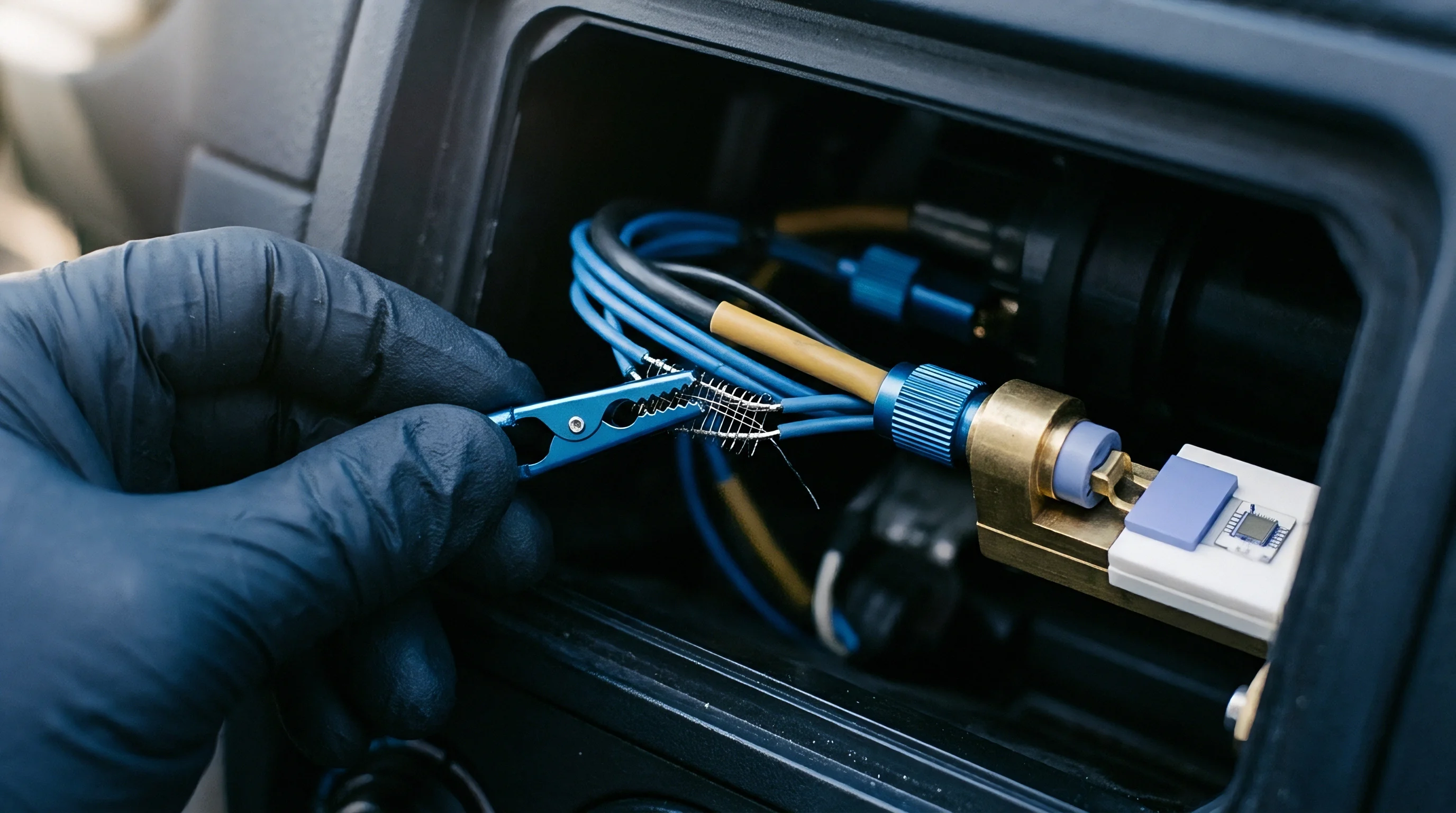
Coaxial shunts utilize a thin-walled cylindrical resistive alloy element housed inside an outer coaxial return conductor. Current enters through the outer housing and flows through the resistive tube to the central signal pickup port. This geometry ensures that magnetic flux generated by current flowing through the resistive element is fully contained within the coaxial structure, preventing stray inductive pick-up from distorting the measured output voltage signal.
The insertion resistance must be kept extremely low, typically between one milliohm and zero point one ohm, to avoid altering the operating dynamics of the pulse driver under test.

Bandwidth Calibration and Probe De-Embedding
Frequency-domain s-parameter characterization isolates probe tip loading effects from true pulsed current signals. Measuring rise times below two nanoseconds requires an instrumentation signal chain with an overall bandwidth exceeding one gigahertz. System rise time is estimated using the root-sum-of-squares calculation, where total system rise time equals the square root of the sum of the square of the driver rise time, the square of the sensor response time, and the square of the oscilloscope rise time.
| Sensor Technology | Upper Bandwidth (-3dB) | Insertion Impedance | DC Response Capability | High-Current Saturation Limit |
|---|---|---|---|---|
| Coaxial Viewing Resistor (CVR) | 2.0 GHz to 3.5 GHz | 0.001 Ω to 0.1 Ω | Full DC Capability | Exceeds 50 kA (Thermal Limited) |
| High-Frequency Rogowski Coil | 100 MHz to 400 MHz | Negligible (<0.1 nH) | No DC Response | Unlimited (Air Core) |
| Pearson Current Transformer | 50 MHz to 200 MHz | Reflected Inductance | No DC Response | Core Saturation at High I-t Product |
| Giant Magnetoresistive (GMR) IC | 10 MHz to 50 MHz | None (Galvanic Isolated) | Full DC Capability | Low Saturation Threshold (<500 A) |
De-embedding techniques remove the frequency-dependent attenuation and phase dispersion introduced by measurement cables, attenuators, and probe interfaces. By acquiring the complex S21 scattering parameters of the signal path using a vector network analyzer, post-processing algorithms invert the channel transfer function to reconstruct the true current pulse profile at the driver terminals.
- Transducer response time must be less than one-third of the target pulse current rise time to prevent signal attenuation.
- Galvanic isolation requirements dictate whether direct-connection coaxial shunts or isolated magnetic loops are integrated into the test fixture.
- Thermal pulse energy handling dictates the maximum allowable action integral of the sensing element during long burst operations.
- Signal-to-noise ratio margins require shielding the transducer against high dv/dt capacitive noise coupling from nearby switching nodes.
According to standard test conditions detailed in MIL-STD-461G clause CS115, pulsed current injection waveforms must be verified into a calibration fixture using a coaxial monitoring probe with a flat frequency response spanning ten kilohertz to one gigahertz.

Sourcing

Commercial Availability and Component Lifecycle Trajectories
Procurement strategies for ultra-fast pulsed components focus on lead-time stability and parasitic parameter consistency across production lots. High-speed power GaN transistors, low-inductance pulse capacitors, and precision coaxial shunts sit in specialized supply pools with limited manufacturing bases worldwide. Single-source dependencies on proprietary wide-bandgap wafer processing lines expose driver manufacturing programs to significant allocation risks when industrial or automotive sectors experience supply chain surges.
Component lot-to-lot parasitic inductance variations in low-cost ceramic capacitors can exceed twenty percent, significantly impacting current rise time consistency in high-volume driver manufacturing.
Qualifying alternative component vendors requires rigorous secondary testing beyond standard datasheet specifications. Dual-sourcing plans must verify that alternate power transistors match primary components in total gate charge, output capacitance, internal gate resistance, and physical package parasitic inductance. Slight variations in lead frame geometry or internal bond wire arrangements between different manufacturers can alter loop inductance by several nanohenries, ruining a tuned high-speed layout.

BOM Cost Distribution for Sub-Nanosecond Drivers
High-frequency capacitor banks and customized low-inductance busbars account for a significant share of assembly line expenses. Standard surface-mount passive components offer low unit prices, but high-power pulsed drivers demand specialty low-ESL reverse-geometry capacitors or RF-grade multilayer porcelain capacitors that command premium unit pricing. Custom laminated busbar assemblies and high-layer-count PCB substrates with sub-100-micrometer dielectric layers further escalate system bill of materials costs.
Power semiconductor switches employing advanced wide-bandgap substrates routinely experience lead times exceeding thirty weeks during supply constraints. To mitigate production halts, sourcing teams establish long-term supply agreements and maintain strategic buffers of critical low-inductance switches and driver ICs. Component lifecycle planning must also track global environmental regulations regarding specialty dielectrics and heavy-metal alloys used in ultra-fast current transducers.
Evaluating total cost of ownership across the driver operational lifespan involves balancing upfront bill of materials investments in ultra-low inductance interconnects against long-term reliability gains achieved through reduced switching stresses and thermal operating margins.