Mechanical Behavior
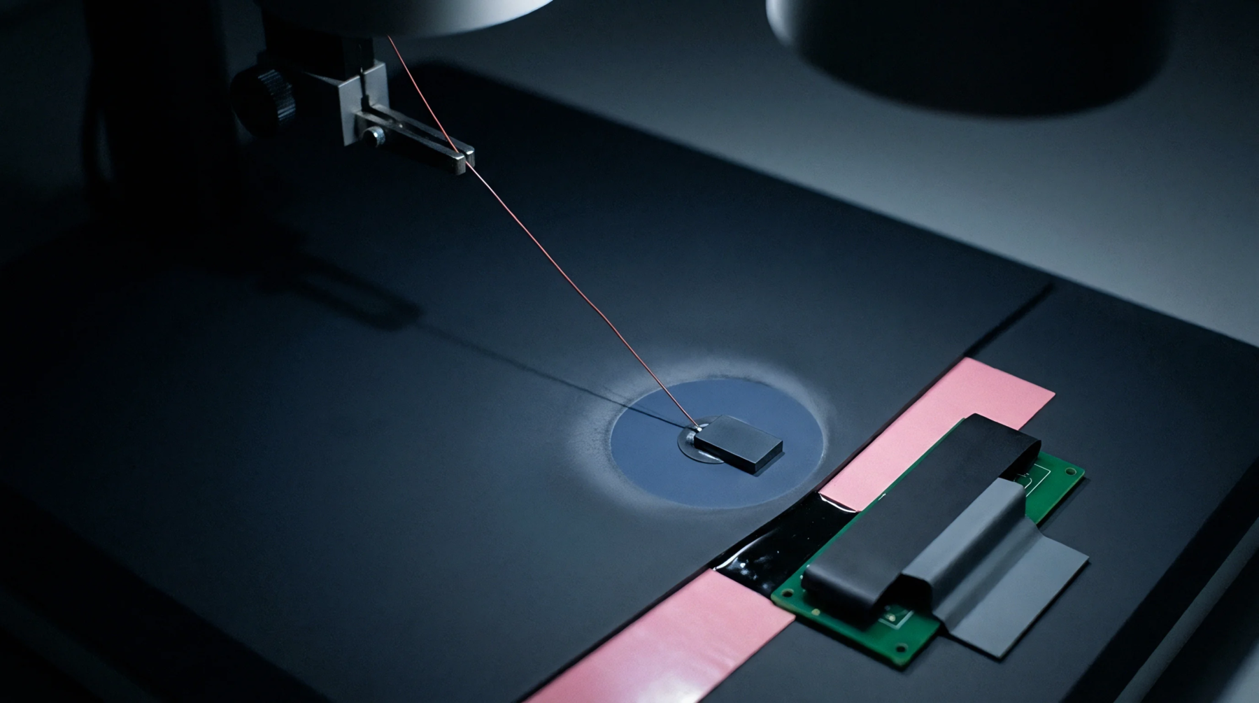
Physical warpage occurs in glass-reinforced epoxy laminates when they are subjected to mechanical forces or thermal cycles during assembly. Such pcb deformation can fracture fragile solder joints and disrupt the alignment of high-precision optical components. The warping behavior is often driven by differences in the thermal expansion coefficients of the copper trace layers and the fiberglass substrate.
Stress Origin
Thermal stress during the solder reflow process is the primary cause of warpage. Uneven copper distribution across the layers leads to unbalanced forces as the board heats. This causes the laminate to twist as it cools.
Failure Mode
The primary consequence of this dimensional change is the failure of surface-mounted ball grid arrays and fine-pitch components. As the board deforms, the solder joints are pulled apart or bridged together, resulting in electrical opens or short circuits. This failure mode can be difficult to detect with automated optical inspection systems alone, often requiring x-ray inspection to confirm.
Prevention Method
Engineers prevent this issue by maintaining a balanced copper distribution across all layers of the board design. Adding stiffener brackets or using high-Tg laminates also reduces the tendency of the board to warp under thermal stress. Simulating the thermal profiles during the design phase allows developers to identify areas of potential stress before manufacturing begins.
This proactive design verification increases the yields of complex assemblies.