Wafer Level Package Land Pattern Stencil Aperture Rules
Fine-pitch WLCSP stencil apertures require area ratios above 0.66, using electroformed foils and rounded square designs to secure clean paste release.

Pitch
Array spacing on wafer level chip scale packages scales from 0.5 mm down to 0.3 mm, compressing copper target diameters to 220 µm with a ±10 µm fabrication variance. Selecting target dimensions for fine-array components requires balancing solder volume against print release stability. When die contacts shrink below 300 µm, standard printed circuit board assembly tolerance bands force explicit trade-offs between bridging prevention and insufficient solder joints.
Bump Dimensioning and Land Pad Ratios
Die surface interconnects feature SAC305 or SAC405 alloy spheres attached to under-bump metallization layers. At 0.4 mm interconnect spacing, a nominal bump diameter of 250 µm matches an underlying board target diameter of 220 µm. Shrinking array spacing to 0.3 mm drops bump diameters to 170 µm, which requires board targets of 150 µm to preserve dielectric insulation channels between adjacent net tracks.
Target surface finish controls liquidus wetting spread during reflow. Electroless nickel immersion gold provides a planar contact planarization layer within ±0.05 µm variation, while organic solderability preservatives introduce zero coplanar variance but require active flux chemistries. Non-solder mask defined configurations isolate copper sidewalls, granting liquid solder a larger physical envelope to envelope the trace geometry during reflow collapse.
SAC305 bump arrays at 0.4 mm centers with 220 µm target pads generate minimum wetting forces when aperture reduction drops below 10 percent.
Board target selection directly alters joint fatigue endurance under thermal cycling. Copper defined targets concentrate stress along top dielectric interfaces. Liquid metal volume determines finished standoff height.
Target expansion increases mechanical endurance while reducing separation distance between adjacent conductive features.

Solder Mask Opening Options
Polyimide mask registration tolerances typically sit at ±25 µm on high-density interconnect layers. Applying solder mask defined targets at 0.4 mm array spacing restricts the exposed metallic contact to 200 µm, creating a boundary ridge that traps flux residues. This ridge alters paste deposit shape during printing, shifting squeegee contact mechanics across package boundaries.
Non-solder mask defined targets remain the primary operational baseline for sub-0.5 mm array spacing. Clearing mask openings by 50 µm beyond copper borders prevents mask overlap caused by registration offset. The exposed copper wall allows molten alloy to coat sidewalls, forming a barrel-shaped interconnect profile upon solidification.
Yield losses decrease when mask clearances maintain uniform perimeter spacing.
| Bump Center Spacing (mm) | Sphere Diameter (µm) | Copper Target Nominal (µm) | Target Tolerance (µm) | Mask Clearance (µm) |
|---|---|---|---|---|
| 0.50 | 300 | 275 | ±12 | 50 |
| 0.40 | 250 | 220 | ±10 | 50 |
| 0.35 | 200 | 180 | ±8 | 40 |
| 0.30 | 170 | 150 | ±5 | 35 |
Copper target size decisions must align with fabrication house capabilities before design sign-off. High-density interconnect fabricators hold tight etch tolerances on 12 µm foil layers. Thicker copper layers expand line width variance.
Etch factor distortions shift circular target profiles into irregular ellipses, altering solder volume calculations. Line edge roughness further impacts wetting integrity.
Engineers evaluate whether array center layout variations can tolerate regional mask misalignments without exposing adjacent signal lines during assembly operations.

Foil
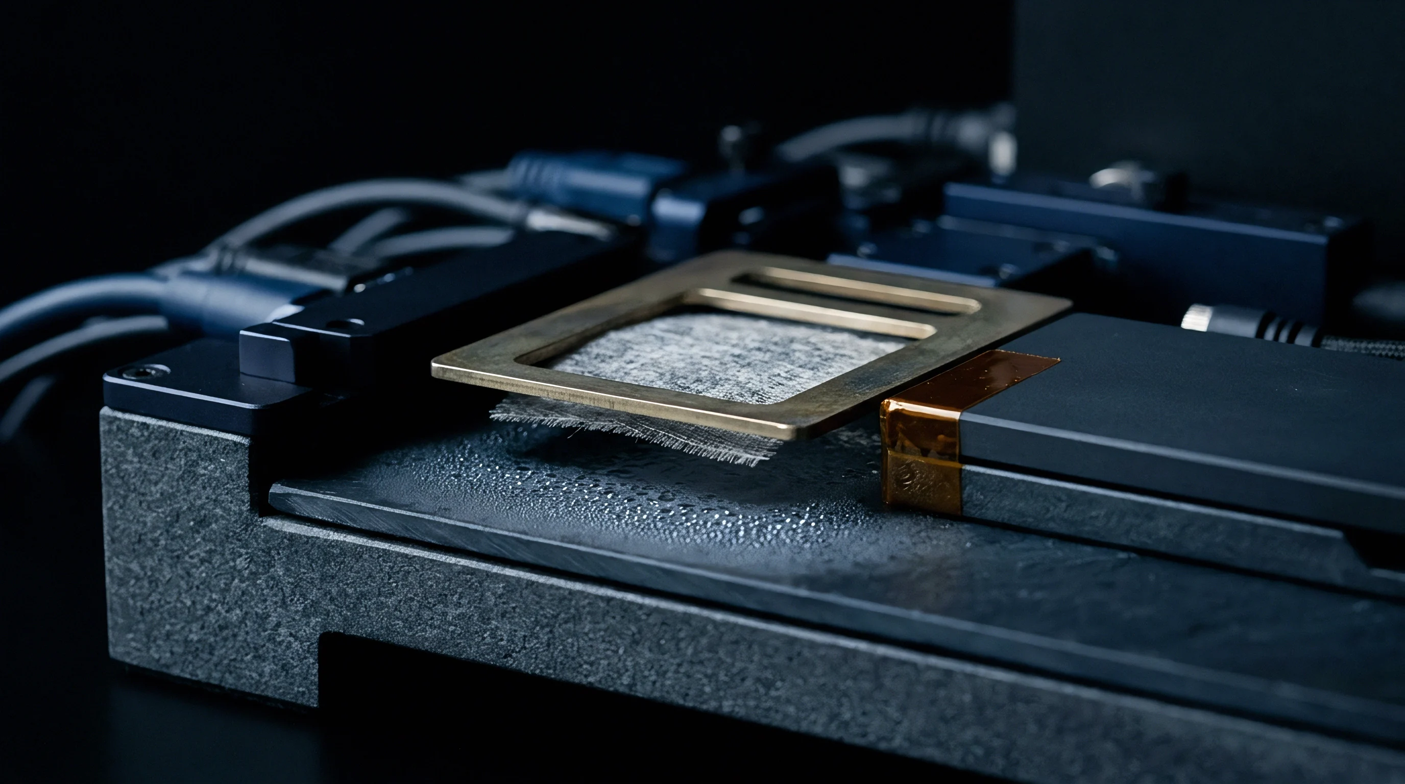
Stainless steel sheets formed through cold rolling serve as the primary raw stock for surface mount printing stencils. Selecting appropriate sheet thickness controls the volume of paste transferred onto high-density land patterns. For package arrays at or below 0.4 mm center spacing, foil thickness defaults to 100 µm or 80 µm to prevent paste clogging inside narrow openings.
Laser Cutting against Electroforming Fabrication
Thermal beam ablation cuts aperture walls with a characteristic taper, producing an entry diameter slightly smaller than the exit diameter. Laser cut opening walls exhibit micro-ridges with peak-to-valley roughness ranging from 1.5 µm to 3.0 µm. This wall texture increases friction against wet solder paste, hindering complete paste transfer on 180 µm apertures.
Additive electroforming constructs metal sheets atom by atom around photoresist pillars, producing nickel foils with smooth aperture walls. Surface roughness on electroformed aperture walls remains below 0.5 µm. The smooth internal boundary reduces paste adhesion, enabling clean paste detachment down to smaller surface area ratios.
Nickel foils also offer superior wear resistance over prolonged print runs.
- Aperture Wall Taper Laser cutting introduces a 5 µm to 8 µm slope across a 100 µm foil thickness, requiring reverse-side squeegee alignment during tool mounting.
- Pasting Paste Release Failure Wall friction exceeding liquid shear strength retains paste inside apertures, leaving starved solder joints on target pads.
- Foil Thickness Mis-Match Mixing 125 µm requirements for large passives with 80 µm WLCSP needs on a single stencil causes uneven squeegee pressure distribution.
- Bridging Under Package Die Excess paste volume transferred through oversized foil thickness bridges neighboring 0.4 mm center contacts during reflow melt.
Foil selection shifts assembly line capability. Electroformed nickel tools cost substantially more than standard laser-cut stainless steel sheets. Production volume dictates whether reduced misprint rates offset initial tooling expense.
High-volume automotive manufacturing runs justify additive nickel tooling. Prototype runs rely on fine-grain laser-cut stainless steel treated with secondary electropolishing processes.
Nano Coating Surface Mechanics
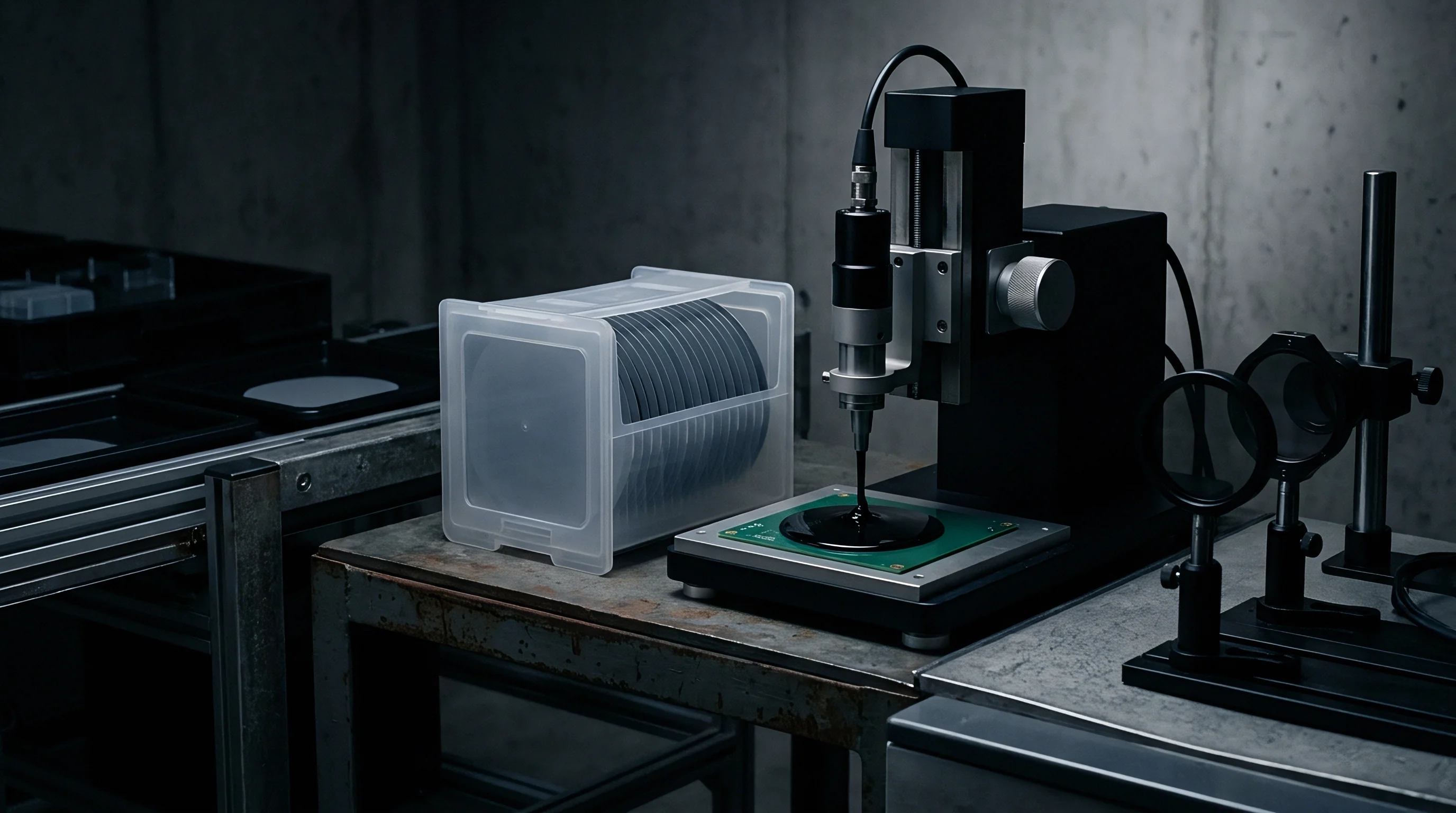
Fluoro-polymeric chemical treatments applied to the contact side of stencil foils alter surface energy dynamics. Hydrophobic and oleophobic nanometer-scale layers prevent solder paste flux binders from adhering to metal undersides. Reduced flux bleeding maintains clean separation between dense aperture patterns during continuous squeegee passes.
IPC-7525B mandates a minimum area ratio of 0.66 for reliable solder paste release from stencil apertures.
Nano-coatings lower cleaning dry-wipe frequency on automatic printers from every five boards to every fifty boards. The liquid flux phase stays inside aperture walls rather than spreading across the underside foil substrate. Surface energy drops from 40 dynes/cm down to below 20 dynes/cm after coating application.
Squeegee blade scrapers move smoothly across coated surfaces, preventing paste smear across 0.35 mm pitch lands.
Coating durability varies across chemistry formulations. Organo-silane coatings withstand roughly 10,000 squeegee cycles before abrasion wears away active surface molecules. Fluoropolymer coatings endure up to 50,000 cycles under controlled squeegee pressure settings.
Line operators monitor print definition decay to identify coating degradation before bridge defects emerge on assembly lines.
Foil selection rules mandate electroformed nickel tools for apertures below 200 µm diameter.


Volume
Calculating paste deposit geometry requires analyzing the ratio between aperture contact area and internal sidewall area. The area ratio metric governs whether liquid alloy separates cleanly from stencil walls during board lowering. When the area ratio drops below 0.66, paste transfer efficiency degrades rapidly, introducing deposit volume fluctuations across the package land pattern.

Which Pitch Threshold Dictates Electroformed Micro-Stencils over Laser Cutting?
Array spacing at 0.35 mm establishes the operational transition point where standard laser-cut stainless steel foils fail to deliver consistent paste deposits. Below this spacing threshold, aperture widths shrink to 180 µm or smaller. Standard laser cutting leaves wall roughness that traps Type 4 solder paste particles, causing volume transfer efficiency to fall below 50 percent.
| Foil Fabrication | Foil Material | Aperture Width (µm) | Area Ratio (AR) | Transfer Efficiency (%) |
|---|---|---|---|---|
| Laser Cut Standard | 304 Stainless Steel | 220 | 0.68 | 78 ±12 |
| Laser Cut Polished | 304 Stainless Steel | 220 | 0.68 | 86 ±8 |
| Electroformed | Pure Nickel | 180 | 0.56 | 91 ±5 |
| Laser Cut Nano | Fine-Grain Steel | 160 | 0.50 | 84 ±7 |
Electroformed nickel micro-stencils maintain transfer efficiency above 85 percent even at an area ratio of 0.55. Smooth nickel sidewalls allow clean particle release during stencil separation. High-density applications operating at 0.3 mm spacing require electroformed foils or nano-coated fine-grain steel to achieve acceptable assembly yields.

Aperture Geometry Math and Reduction Ratios
Designing openings for circular target pads requires choosing between round and square aperture geometries. Square apertures offer a larger surface area for a given width dimension, increasing the area ratio compared to circular openings. However, solder paste release can stall in sharp 90-degree corners, leading to incomplete deposit formation.
- Calculate circular target area using target diameter and standard manufacturing tolerances.
- Determine candidate aperture shape, applying corner radii of at least 60 µm to square geometries.
- Compute sidewall surface area based on selected stencil foil thickness.
- Divide top opening area by internal sidewall area to verify the area ratio exceeds 0.66.
- Apply percentage reduction rules to adjust final deposit volume relative to copper target size.
Square apertures with rounded corners maximize area ratio values while maintaining smooth paste detachment. For a 220 µm circular target pad on a 100 µm stencil foil, a 220 µm square aperture with 50 µm corner radii yields an area ratio of 0.71, compared to 0.55 for a matching circular aperture. Corner rounding prevents paste entrapment while providing sufficient solder paste volume to form reliable interconnect joints.
Aperture reduction rules balance bridging mitigation against joint starvation risk. Reducing aperture dimensions by 10 to 15 percent relative to copper target pads provides a buffer against print misalignments. For 0.4 mm center packages, a 220 µm target pad pairs with a 200 µm rounded square aperture, yielding stable deposit heights without paste squeeze-out during component placement.

Type 4 and Type 5 Paste Release Behavior
Particle size distribution within solder paste formulations directly affects release dynamics through narrow aperture openings. Type 4 paste features powder spheres measuring between 20 µm and 38 µm in diameter. Type 5 paste reduces sphere size down to a range of 15 µm to 25 µm, improving packing density within micro-apertures.
Printing Type 4 paste through apertures smaller than 200 µm causes particle bridging across the opening, restricting paste ingress during squeegee passes. Industry guidelines mandate that aperture width span at least five average particle diameters to ensure smooth paste flow. Type 5 paste satisfies this particle packing requirement for aperture widths down to 125 µm, making it the standard choice for 0.3 mm array spacing layouts.
Switching from Type 4 to Type 5 paste increases susceptibility to metal powder oxidation due to the larger aggregate surface area of smaller spheres. Assembly facilities control ambient room humidity and reflow atmosphere parameters to counter oxidation risks. Nitrogen inerting during reflow reduces solder balling and promotes complete wetting across fine-pitch target structures.
Deviating from area ratio minimums produces deposit volume variations that trigger tombstones, open circuits, and bridging defects during reflow operations.


Trace
Routing signal lines away from high-density package arrays requires precise trace geometry selection to avoid altering pad thermal capacity. Asymmetrical copper connections draw thermal energy away from pads at uneven rates during reflow heating. This thermal imbalance causes unequal solder melting timing, pulling the component off center alignment.

Asymmetrical Copper Routing and Thermal Pull
Connecting a wide power trace directly to one target pad while thin signal lines connect to adjacent pads creates a thermal gradient across the array layout. Solder on the thermally isolated pads reaches liquidus temperature first, melting and exerting surface tension forces before the power pad completes reflow. This asymmetrical force balance pulls the package die out of position, causing open contacts or bridging failures.
Neck-down routing techniques balance thermal dissipation rates across all package contacts. Power tracks shrink to match signal line widths within a 300 µm distance from target perimeters. Solder mask dams isolate copper traces from pads, preventing liquid metal from wicking down signal lines during reflow melt.
Standard neck-down dimensions cap trace width entry at 50 percent of target pad diameter.
Standard IPC-2221 design rules mandate neck-down trace widths within 300 µm of fine-pitch target pads to prevent thermal imbalance during reflow.
Equalizing copper mass around array contacts stabilizes thermal behavior during soldering cycles. Solid ground planes beneath package footprints require thermal relief cutouts around target vias to prevent rapid heat dissipation. Balanced routing geometries ensure simultaneous solder melt across all array contacts, maintaining component position accuracy.

Under-Pad Micro-Via Offsets
High-density interconnect designs place micro-vias directly within target lands to eliminate external escape trace routing. Blind micro-vias formed via laser ablation connect layer one copper targets to layer two signal tracks. Unfilled micro-vias create small cavities within target centers, drawing liquid solder away from main joint structures during reflow.
Micro-via diameter selection dictates whether filling and planarization steps are necessary prior to surface mounting operations. Vias smaller than 75 µm diameter can accept direct soldering when paired with high-viscosity paste chemistries. Larger micro-vias require copper plating fill processes to create flat, planar targets that prevent solder voiding and volume depletion during reflow operations.
Off-center micro-via placement within target pads distorts solder paste release and reflow dynamics. Via captures positioned near pad edges disrupt surface tension symmetry during solder collapse, causing package tilt. Fabrication rules specify micro-via center location tolerances within ±10 µm of land center points to preserve joint symmetry across the array layout.
Suppliers often attribute array assembly bridging defects to PCB fabrication tolerances rather than acknowledging stencil misregistration errors during paste printing.

Loss
Automated optical inspection systems inspect solder paste deposit height, area, and volume prior to component placement operations. Establishing realistic inspection thresholds prevents unnecessary line stops while catching true misprint defects. For 0.4 mm center package arrays, volume control limits sit at ±20 percent of theoretical aperture design volume.
Assembly Yield and Inspection Boundaries
Post-reflow inspection relies on 3D X-ray systems to evaluate hidden interconnect structures underneath silicon die components. Solder joint void limits follow IPC-A-610 criteria, capping total void area at 25 percent of the total interconnect footprint. Individual voids larger than 10 percent of the pad area trigger joint reliability failures due to mechanical stress concentration risks.
Coplanar alignment tolerances across package arrays dictate acceptable substrate flexure limits during reflow processing. Substrate warping exceeding 50 µm across a 5 mm die footprint induces open joints on corner contacts. High-temperature substrate materials with matching coefficients of thermal expansion minimize warping forces during assembly profiles.
Rework procedures for fine-pitch array components require specialized hot-air profile tools and localized vacuum pick-up heads. Removing defective packages requires applying uniform heat profiles to prevent thermal damage to neighboring parts. Board surface preparation includes mechanical solder clearing and fresh flux application before landing replacement components.
IPC-J-STD-001 Class 3 standards mandate complete wetting across target sidewalls with zero solder bridging between adjacent fine-pitch array contacts.