Solid State Intermetallic Growth Mechanisms during Terminal Baking
Terminal baking converts Cu6Sn5 to Cu3Sn via parabolic solid-state diffusion, driving Kirkendall voiding and sensor strain shift unless nickel barrier plating limits compound growth.


Phase
Isothermal baking between 125°C and 175°C drives solid-state atom diffusion across metal boundaries in surface-mount assemblies. These reaction kinetics operate continuously during post-assembly processing, moisture baking, and thermal testing. Copper and tin atoms migrate across solder interfaces at rates set by lattice vacancy concentrations and thermal activation energy, forming structural intermetallic compounds without liquid solder.
Diffusional transport in copper-tin solder systems produces two primary intermetallic structures. Solder reflow initially establishes the tin-rich eta phase (Cu6Sn5), which subsequent thermal baking converts through solid-state reactions into the copper-rich epsilon phase (Cu3Sn). Growth follows parabolic diffusion relationships, where compound thickness increases with the square root of thermal exposure time.
Activation energy for solid-state epsilon phase growth ranges from 0.85 to 1.05 electron-volts. Because tin diffuses faster than copper, high thermal baking accelerates copper dissolution into the bulk solder matrix, doubling the reaction rate for every fifteen-degree rise in processing temperature and continuously consuming substrate metal.

Isothermal Kinetics in Lead Free Solder Interconnects
Thermal activation accelerates tin and copper atomic migration long after primary reflow solidification finishes. In lead-free alloys ~ specifically tin-silver-copper formulations like SAC305 ~ solid-state interfacial growth kinetics exhibit distinct parabolic rate constants during component storage baking. Thermal exposure at 150°C generates compound growth rates between 0.05 and 0.12 micrometers per square-root hour.
A 125°C moisture bake yields slower accumulation, whereas 175°C burn-in processing accelerates interface conversion dramatically.
Standard parabolic diffusion equations govern overall layer expansion across operational temperature bands. The total compound thickness w at time t depends on initial layer thickness w0 and the temperature-dependent diffusion coefficient D:
w(t) = w0 + (D t)^0.5
The diffusion coefficient follows Arrhenius behavior based on the pre-exponential factor D0, activation energy Q, Boltzmann constant k, and absolute temperature T:
D = D0 exp(-Q / (k T))
Evaluating activation energy across lead-free formulations reveals that copper-tin compound growth demands lower thermal energy than nickel-tin growth. Consequently, direct solder attachments on bare copper leadframes experience faster interfacial layer thickening during baking than connections made on nickel-plated substrates.

Solid State Conversion of Intermetallic Layers
At baking temperatures above 100°C, the copper-rich epsilon layer grows at the direct expense of the tin-rich eta structure. The solid-state transformation consumes eta-phase Cu6Sn5 and underlying copper base metal according to a fixed stoichiometric reaction:
Cu6Sn5 + 9 Cu -> 5 Cu3Sn
This solid-state transformation reorganizes crystal lattices at the substrate interface. At baking temperatures, the eta phase possesses a monoclinic crystal structure, whereas the epsilon phase forms an orthorhombic lattice. Shift between these different crystal symmetries creates localized lattice strain along the interfacial boundary.
Long thermal baking cycles alter the relative thickness proportion between Cu6Sn5 and Cu3Sn. Immediately after reflow, Cu6Sn5 accounts for over ninety percent of total intermetallic thickness, but extended baking at 150°C for one hundred hours converts the interface until Cu3Sn dominates the substrate junction. Because the epsilon phase exhibits higher elastic modulus and greater hardness than the eta phase, this shift increases interfacial brittleness under subsequent mechanical strain.
A 100-hour bake at 150°C expands the sub-micron boundary layer into a continuous three-micron band, permanently altering mechanical compliance.


Void
Structural defects originate when atomic flux divergence creates uncompensated movement of lattice vacancies. Unequal diffusion rates across binary metal interfaces generate vacancy accumulation during solid-state thermal aging. In copper-tin systems, copper atoms diffuse out of the substrate lattice into the Cu3Sn intermetallic layer substantially faster than tin diffuses back, leaving excess vacancies in the copper base metal that reach supersaturation and condense into microscopic voids.
Vacancy coalescence occurs primarily along the boundary between the copper substrate and the Cu3Sn intermetallic layer. These Kirkendall microvoids reduce the net physical contact area across the solder joint interface. Interfacial shear strength drops sharply as void density increases.
Thermal baking duration directly dictates total vacancy volume accumulation, where prolonged high-temperature baking transforms isolated microvoids into continuous planar planar lines, predisposing solder joints to brittle mechanical fracture under minimal stress.
Kirkendall Vacancy Coalescence at Copper Interfaces
Diffusional asymmetry between copper and tin drives lattice transport during extended thermal exposure. Direct copper substrates exposed to 150°C terminal baking experience active vacancy injection into the substrate lattice. Secondary factors ~ including organic brighteners in electroplated copper, sulfur impurities, and residual hydrogen gas ~ accelerate vacancy clustering.
Consequently, high-purity rolled annealed copper exhibits lower vacancy condensation rates than electrodeposition copper finishes under identical baking profiles.
A 150°C terminal bake exceeding 96 hours on direct copper substrates produces an average Kirkendall void area fraction above twelve percent along the epsilon-phase boundary.
Quantifying vacancy distribution requires secondary ion mass spectrometry and high-resolution electron microscopy. When void area fraction along the interfacial boundary surpasses fifteen percent, mechanical drop shock durability decreases by more than fifty percent, while thermal cycling life drops concurrently due to localized stress concentrations surrounding individual void clusters.

Electroless Nickel Phosphorus Degradation Sequences
Plating formulations containing nickel and electroless phosphorus generate distinct microstructural degradation paths under heat. Electroless Nickel Immersion Gold (ENIG) and Electroless Nickel Electroless Palladium Immersion Gold (ENEPIG) finishes rely on a nickel-phosphorus barrier layer containing seven to eleven weight percent phosphorus. During high-temperature terminal baking, tin diffuses through the thin gold layer to react with nickel, forming the Ni3Sn4 intermetallic phase.
| Surface Finish | Dominant Intermetallic Phase | Growth Constant (um/hr^0.5) | Interfacial Defect Mode | Critical Bake Limit (Hours) |
|---|---|---|---|---|
| Bare Copper (SAC305) | Cu6Sn5 / Cu3Sn | 0.085 | Kirkendall Microvoiding | 96 |
| ENIG (Ni-P / Au) | Ni3Sn4 / Ni3P | 0.022 | Phosphorus-Rich Bi-Layer Brittle Spalling | 168 |
| ENEPIG (Ni-P / Pd / Au) | (Pd,Ni)Sn4 / Ni3Sn4 | 0.018 | Ternary Hyper-Eutectic Phase Segregation | 240 |
| Immersion Tin | Cu6Sn5 | 0.092 | Substrate Consumption / Tin Whisker Nucleation | 48 |
Nickel consumption during Ni3Sn4 growth rejects phosphorus into the remaining nickel substrate. Because phosphorus has negligible solubility in Ni3Sn4, it accumulates at the reaction interface as a brittle, high-phosphorus Ni3P bi-layer. Extended thermal baking expands this zone into a secondary ternary Ni-Sn-P phase band, resulting in high residual tensile stress and poor fracture toughness.
- Boundary Separation occurs when coalesced vacancy arrays weaken mechanical shear strength below thirty megapascals.
- Phosphorus Accumulation forms a brittle nickel-phosphide layer directly beneath the tri-metallic intermetallic matrix.
- Solderability Degradation develops when tin consumption exhausts the active surface layer, exposing non-wettable intermetallics.
- Cratering Fractures propagate along stress concentration sites during subsequent package assembly handling.
Ignoring vacancy formation kinetics during extended bake cycles results in field shear failures under routine operational vibration.
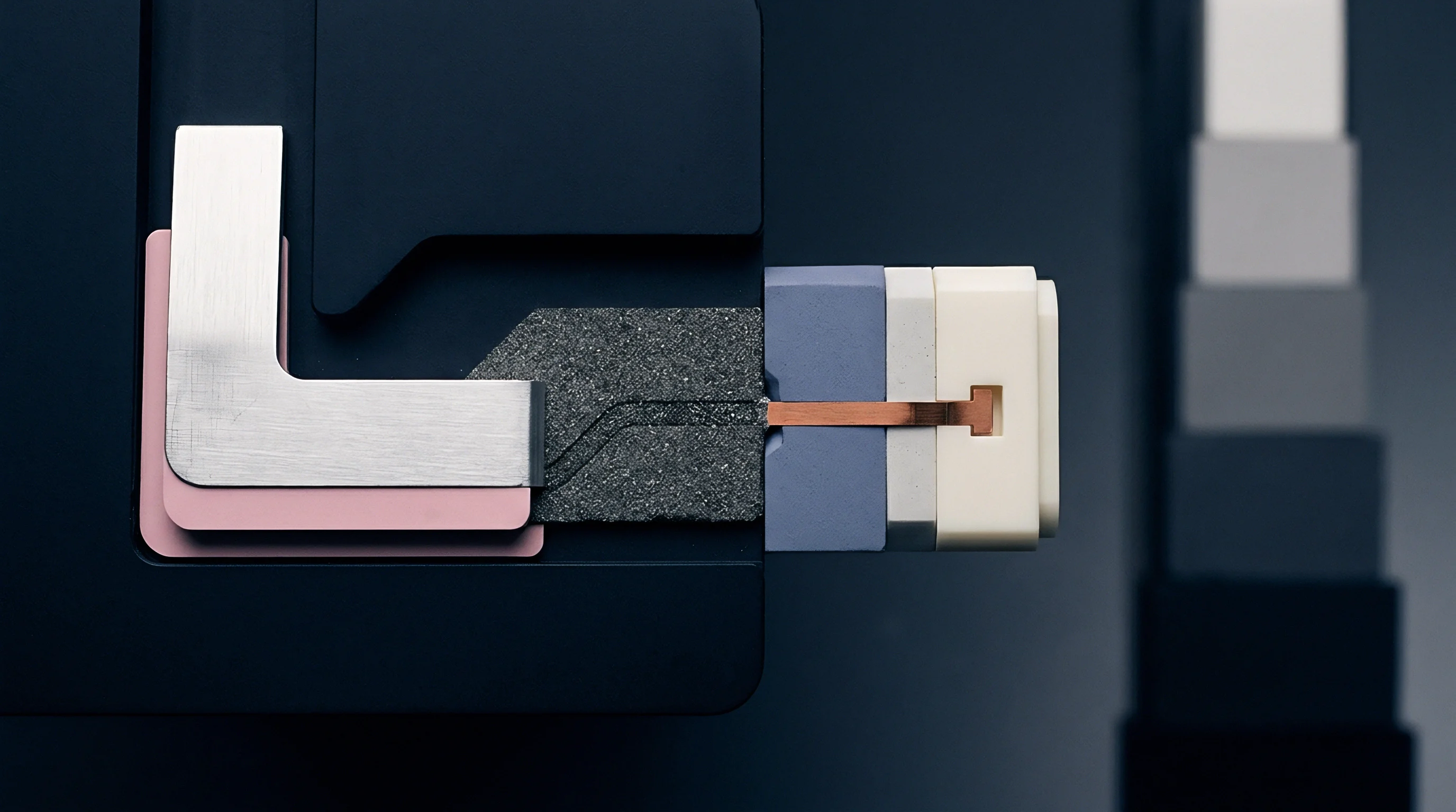

Offset
Mechanical strain generated by volume changes in solid-state reaction products alters sensor baseline electrical outputs. Molar volume differences between base metals and their corresponding intermetallic compounds induce significant localized stresses during solid-state growth. When bare copper converts to Cu6Sn5, molar volume expands; subsequent conversion of Cu6Sn5 and copper into Cu3Sn results in a net volumetric contraction of approximately 5.2 percent within the reaction zone.
This localized volumetric contraction generates high residual tensile stresses within underlying traces and die-attach pads. In precision analog sensing elements, piezoresistive MEMS devices, and optical sensors, package-induced stress transfers directly into the silicon substrate. Shifting digital counts upward, solder joint stress fields cause zero-point output drift, sensitivity calibration errors, and uncompensated offset hysteresis over component lifetime.

Package Stress Evolution and Die Attach Strain
Molar volume discrepancies between base metals and intermetallic compounds create localized tensile stress fields within package substrates. Solid-state conversion during a 150°C terminal bake shifts the mechanical stress distribution across silicon die attachments. For a 3 mm by 3 mm piezoresistive pressure sensor die attached with SAC305 solder on a copper leadframe, a 96-hour bake converts 1.5 micrometers of interfacial copper into Cu3Sn, inducing a compressive stress shift of up to 18 megapascals across the bottom surface of the die.
Compliance with IPC J-STD-020 moisture sensitivity bake limits prevents uncalibrated analog zero-point shifts exceeding one percent of full scale output.
Transferred compressive stress warps the delicate sensing diaphragm inside MEMS structures. An 18-megapascal interfacial stress change alters the zero-point voltage of a silicon Wheatstone bridge by +1.4 percent of full-scale output span. In a 16-bit digital sensor front-end, this mechanical shift alters baseline reading by 917 counts.
Sensor compensation algorithms hardcoded into host firmware before terminal baking fail to correct for post-bake mechanical offset changes, producing persistent measurement errors on the host communications bus.

Contact Resistance Instability in Bus Interface Pins
High-density interconnect pins experience micro-scale mechanical displacement as intermetallic layers consume the underlying copper traces. In surface-mount packages featuring small-pitch I2C or SPI communication pins ~ such as Quad Flat No-Lead (QFN) or Land Grid Array (LGA) forms ~ intermetallic growth degrades electrical conductivity. While bulk copper exhibits an electrical resistivity of 1.7 microhm-centimeters, Cu6Sn5 displays a resistivity of 17.5 microhm-centimeters and Cu3Sn measures 8.9 microhm-centimeters.
Extensive consumption of thin copper trace plating by high-resistivity intermetallic phases increases pin series resistance. On high-speed SPI signal lines operating above 10 megahertz, increased contact resistance combines with parasitic bus capacitance to round signal edge transitions. Rising edge delays degrade timing margins, causing frame errors and packet drops on digital buses.
Ground pad intermetallic degradation similarly introduces ground-bounce noise, destabilizing internal analog-to-digital converter reference voltages inside integrated sensor packages.

Audit
Verification of interfacial layer integrity demands non-destructive testing combined with cross-sectional electron microscopy. Physical characterization confirms whether terminal baking parameter boundaries preserve intermetallic boundaries within accepted limits. Qualification protocols evaluate structural integrity before releasing baked component lots to surface-mount production lines.
Metallographic analysis provides definitive quantification of compound phase thickness and vacancy defect density. Because optical microscopy lacks sufficient magnification to resolve sub-micron Cu3Sn layers and Kirkendall microvoids, analytical facilities employ Field Emission Scanning Electron Microscopy (FE-SEM) paired with Energy Dispersive X-ray Spectroscopy (EDX). Acoustic microscopy complements electron beam methods by non-destructively scanning internal package interfaces for bake-induced delamination.

How Does High Temperature Bake Accelerate Interfacial Voiding?
Elevated thermal energy increases vacancy concentration while accelerating atomic movement across the intermetallic boundary. Higher temperatures exponentially expand atomic jump frequencies within metal crystal lattices. As ambient temperature approaches the absolute melting point fraction of solder alloys, intrinsic vacancy concentration rises according to thermodynamic equilibrium.
Uncompensated atomic transport across the boundary injects surplus vacancies into the substrate at rates far exceeding room-temperature relaxation mechanisms.
Cross-sectional examination reveals microstructural degradation long before electrical continuity testing detects circuit open failure.
Quantifying thermal acceleration requires testing components under controlled isothermal storage profiles specified in JESD22-A103. Test conditions ranging from Condition A (125°C) to Condition C (175°C) establish empirical acceleration factors for specific solder alloy and substrate plating combinations.

Cross Sectioning and Microstructural Characterization Standards
Metallographic preparation requires careful mechanical polishing and selective chemical etching to preserve sub-micron intermetallic structures. Improper techniques ~ such as aggressive polishing or incorrect diamond suspension slurry sizing ~ smear soft solder across hard intermetallic boundaries, obscuring microvoids.
| Inspection Method | Target Anomaly | Detection Resolution | Standard Protocol | Acceptance Threshold |
|---|---|---|---|---|
| Acoustic Microscopy (C-SAM) | Die-Attach Delamination / Large Voids | 1.0 micrometer | JESD22-A104 | Zero interfacial delamination area > 10% |
| Field Emission SEM | Cu3Sn / Cu6Sn5 Layer Thickness | 5.0 nanometers | IPC-TM-650 2.1.1 | Total IMC thickness < 4.0 micrometers |
| EDX Spectroscopy | Elemental Phase Identification | 0.1 atomic percent | ASTM E1508 | Stoichiometric Cu3Sn and Cu6Sn5 verification |
| Wetting Balance Testing | Solderability Degradation | 0.01 millinewtons | J-STD-003 | Zero-cross time < 1.0 second post-bake |
Preparing samples for analytical inspection involves a sequential metallurgical grinding and etching process to isolate structural boundaries accurately.
- Mount the post-bake package component in clear acrylic cold-curing epoxy resin under vacuum backfill.
- Grind down to the primary interconnect row using silicon carbide abrasive papers from 400 to 4000 grit.
- Polish the specimen surface with diamond suspensions down to one-quarter micron particle size.
- Etch the metallographic surface using an ammonium hydroxide and hydrogen peroxide solution for three seconds.
- Measure intermetallic layer thickness and vacancy area fraction under secondary electron imaging at ten thousand times magnification.
Accurate cross-sectioning confirms whether interfacial intermetallic growth exceeds industrial reliability limits. JESD22-A103 Method B specifies continuous high temperature storage testing at 150°C, requiring hardware suppliers to demonstrate intermetallic stability prior to qualification sign-off.


Scrap
Thermal regeneration of floor-life expired components introduces commercial trade-offs between packaging material damage and inventory write-offs. Moisture-sensitive surface-mount devices exceeding allowable exposure limits under IPC/JEDEC J-STD-033 demand high-temperature baking before reflow assembly. Subjecting components to 125°C moisture removal bakes resets floor-life clocks but consumes finite thermal budget allowances.
Baking component inventory inside original carrier packaging presents operational risks. Polystyrene carrier tapes, anti-static cover ribbons, and plastic shipping reels melt or warp when exposed to temperatures exceeding 60°C. Because standard carrier tape cannot withstand 125°C moisture bakes, manufacturing operators must transfer components manually onto high-temperature metallic trays prior to baking. Yield losses reach three percent during manual transfer due to bent leads and electrostatic discharge events.

Tape and Reel Packaging Thermal Constraints
Polystyrene carrier tapes and anti-static cover ribbons suffer thermal deformation when subjected to baking temperatures above sixty degrees Celsius. Standard carrier tape materials soften, causing pocket collapse and component locking. Outgassing plasticizers from heated carrier tapes deposit chemical films onto lead finishes, severely degrading post-bake solderability.
Re-baking surface mount components inside plastic tape carrier pockets causes cover tape adhesive transfer and feeder pickup failure.
High-temperature specialty carrier tapes fabricated from polyetherimide or modified polycarbonate withstand 125°C baking without dimensional distortion. However, these high-temperature materials increase packaging unit costs by 30 to 50 percent, so buyers must balance the up-front cost premium of bakeable carrier tape against potential labor costs and yield losses incurred during manual tray transfer.

Yield Loss Arithmetic across Terminal Storage Cycles
Calculating the total financial cost of moisture removal requires evaluating component unit price against assembly line downtime risks. Low-cost discrete passive components rarely justify high-temperature baking; scrapping expired inventory proves more economical than paying operator labor costs for tray transfer and baking cycles.
| Package Type | Unit Price Range (USD) | Bake Temperature / Time | Carrier Tape Rating | Break-Even Action Threshold |
|---|---|---|---|---|
| Fine Pitch QFN (MSL 3) | 0.45 – 1.20 | 125°C / 24 Hours | Standard Polypropylene (60°C Max) | Scrap lots under 500 units; bake larger lots |
| High-Density BGA (MSL 4) | 12.50 – 85.00 | 125°C / 48 Hours | High-Temp Polycarbonate (125°C Max) | Bake directly in tape; zero transfer scrap |
| MEMS Sensor Module (MSL 5) | 3.20 – 8.50 | 90°C / 72 Hours | Low-Deformation PEI (100°C Max) | Bake at reduced temp to protect calibration |
| 0402 Passive Array (MSL 2) | 0.005 – 0.020 | 125°C / 12 Hours | Paper / Polystyrene (55°C Max) | Scrap immediately upon floor-life expiration |
Deciding whether to authorize terminal baking cycles on aged component inventory relies on a structured engineering evaluation.
- Thermal Rating Verification confirms whether carrier tape polymers survive target baking temperatures without dimensional distortion.
- Terminal Oxidation Assessment evaluates lead finish discoloration following extended thermal cycles prior to line loading.
- Intermetallic Accumulation Modeling predicts cumulative thermal exposure to ensure total compound growth stays below two micrometers.
- Feeder Machine Compatibility checks post-bake tape mechanical tolerances to prevent pick-and-place nozzle mispicks.
Whether low-temperature vacuum desiccation can eliminate moisture without triggering solid-state diffusion kinetics remains a subject of ongoing commercial trials.


Contract
Procurement specifications establish strict quantitative limits on pre-assembly thermal history and plating layer thickness. Sourcing agreements for integrated circuits and surface-mount sensor modules must dictate maximum permitted intermetallic compound growth prior to customer receipt. Uncontrolled thermal baking by distributors or contract manufacturers consumes critical thermal budget, delivering parts with advanced interfacial degradation.
Contractual terms define acceptable leadframe plating structures, diffusion barrier requirements, and maximum cumulative bake times. Requiring suppliers to incorporate nickel diffusion barriers beneath matte tin or gold surface finishes retards solid-state copper transport. Sourcing clauses define explicit lot rejection thresholds based on wetting balance performance and metallographic cross-section analysis.
Leadframe Plating Specifications for Thermal Resilience
Enforcing a minimum nickel barrier thickness protects underlying copper leadframe material from rapid tin consumption during baking. Direct tin plating on copper leadframes leads to rapid Cu6Sn5 and Cu3Sn accumulation during storage, whereas an electroplated nickel underlayer with a minimum thickness of 1.27 micrometers creates an effective atomic diffusion barrier.
Solid-state diffusion of nickel into tin proceeds at less than one-fifth the rate of copper into tin at 150°C. Sourcing documentation specifying ENIG or ENEPIG finishes must stipulate strict nickel deposit phosphorus content between 7.0 and 9.0 weight percent to mitigate brittle Ni3P phase formation during mandatory terminal baking.

RFQ Guardrails for Intermetallic Growth Limits
Request for quotation documents define maximum acceptable intermetallic boundary thickness before component delivery. Purchasing specifications must cap pre-delivery intermetallic layer thickness at 0.5 micrometers for fresh components. This requirement preserves sufficient unreacted copper and tin substrate volume to sustain multiple reflow passes and subsequent MSL reset bakes without inducing Kirkendall voiding.
Incorporate explicit clauses into supply agreements requiring vendors to report all thermal processing history, including burn-in parameters, factory drying bakes, and reel repackaging dates. Component lots subjected to unauthorized re-baking exceeding 48 cumulative hours at 125°C face immediate rejection at incoming quality receiving. Suppliers providing leadframes with robust diffusion barrier layers deliver consistent solderability regardless of terminal baking history.