Surface Mount Housing
Quad-flat no-lead housings utilize a plastic-encapsulated leadframe with peripheral pads on the bottom surface of the body. Designing circuits with QFN Packaging provides high thermal dissipation and low electrical inductance due to the direct board connection through a large exposed center pad. The absence of long leads reduces the overall footprint and weight of the integrated circuit.
Assembly Challenge
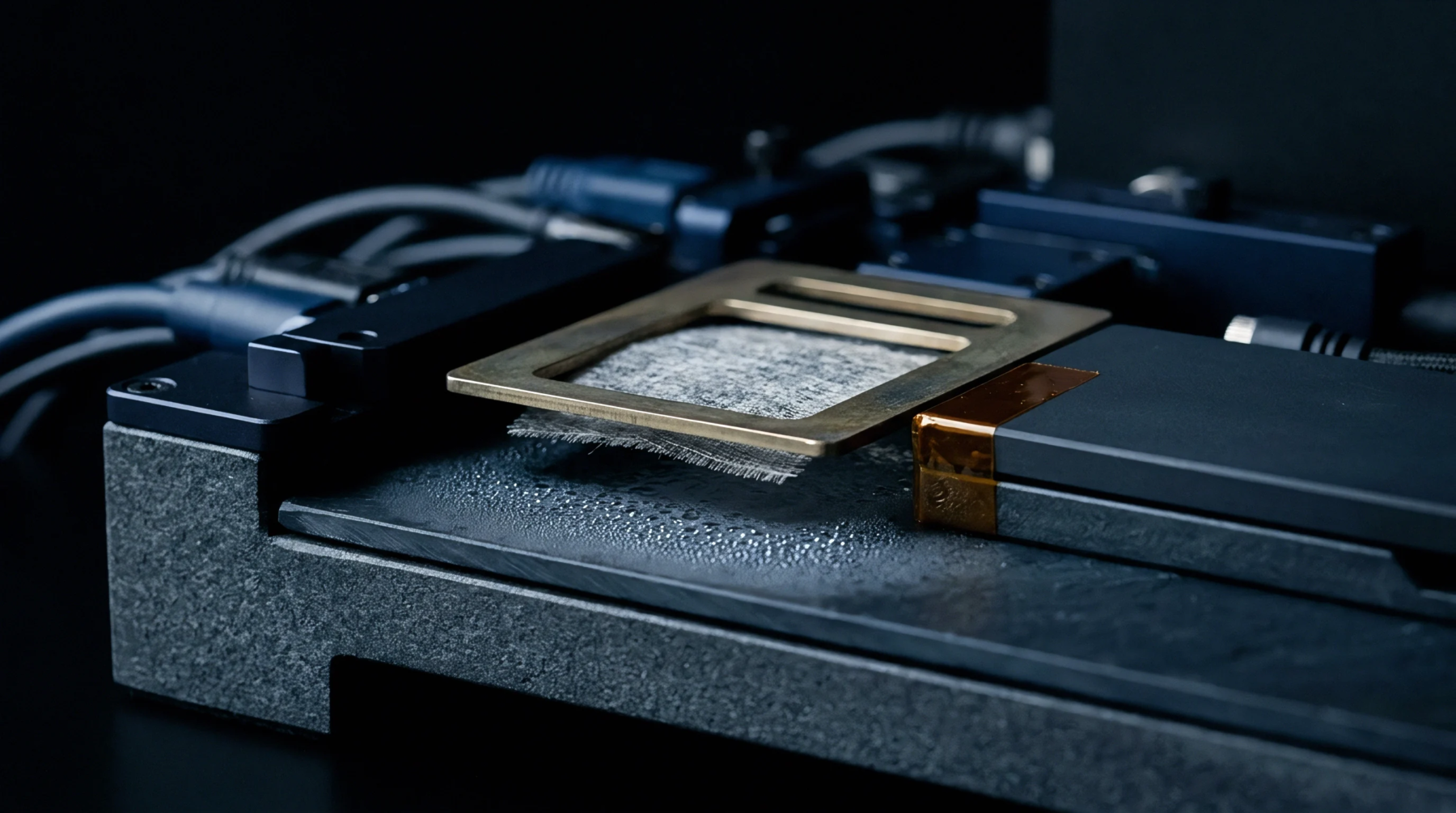
Soldering the central pad requires careful control of the solder paste volume to prevent the component from floating on a dome of molten alloy. If too much paste is applied, QFN packaging can tilt during reflow, which lifts the peripheral leads off their pads and causes open circuits. Using segmented stencil apertures reduces the paste volume while ensuring a reliable thermal and electrical connection to the board.
Thermal Transfer
The exposed pad is soldered directly to a copper land on the board, which connects to internal ground planes through thermal vias. This arrangement allows heat to flow from the silicon die to the board with minimal thermal resistance.
Visual Inspection
Peripheral solder joints are located underneath the package body, making standard visual inspection difficult. Using transmission x-ray inspection or automated optical inspection is necessary to verify the quality of the solder connections.