
Viscoelastic Shear Relaxation in Surface Mount Sensor Packaging Substrates
Substrate viscoelastic shear relaxation drives post-reflow sensor zero-point drift, requiring high-Tg resins, strain-decoupled pads, or host software recalibration.
Substrate viscoelastic shear relaxation drives post-reflow sensor zero-point drift, requiring high-Tg resins, strain-decoupled pads, or host software recalibration.

Optimizing stencil apertures and thermal profiles prevents tombstoning, solder voiding, and calibration shift in reflowed discrete sensors.

Lithographic die shrinks require simultaneous nozzle, stencil, and register map updates to prevent continuous SMT line stoppages during manufacturing transitions.

Silicon stepping registers provide unambiguous hardware verification, ensuring firmware driver compatibility and protecting production lines from unannounced die alterations.
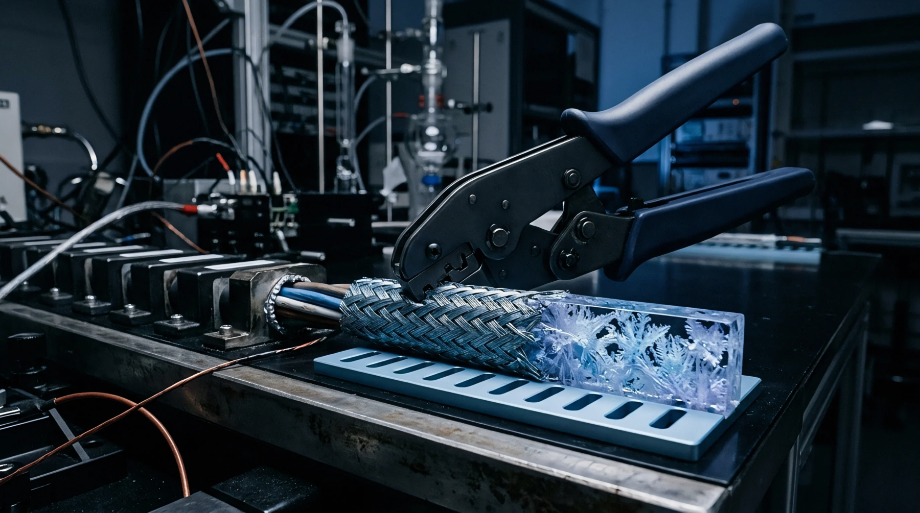
Asymmetric clamping torque on pressure port glands induces anisotropic diaphragm strain, driving piezoresistive zero shift that digital calibration cannot isolate.

Analytical strain attenuation models quantify flexural stress transfer through solder lands, enabling optimized patterns that prevent sensor drift and joint fatigue.
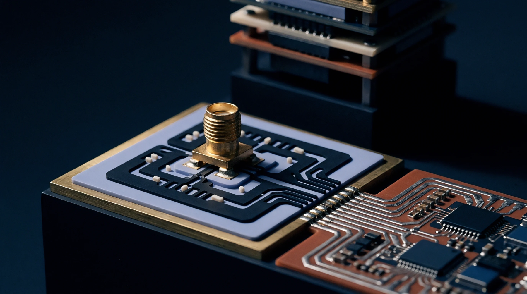
Precision PCB stress relief requires milled isolation slots around sensitive packages alongside symmetrical non-solder-mask-defined land patterns.

Common centroid geometry eliminates linear gradients in precision silicon references, transferring residual drift limits entirely to packaging stress and bus trim.
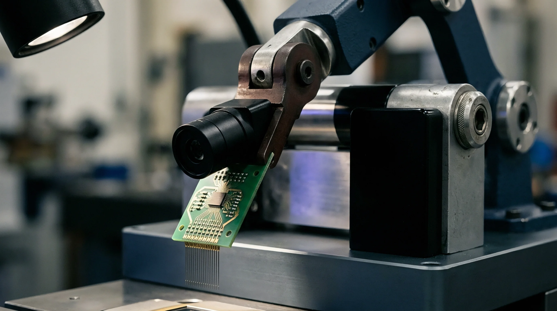
Lead-free solder solidification locks high shear stress into piezoresistive dies, requiring compliant packages or post-reflow dwell times to stabilize zero-point drift.

Hardware I2C multiplexers isolate identical peripheral addresses and split capacitive loads across independent, switchable bus branches.

Dynamic sensor address resolution in high-noise arrays requires differential physical-layer isolation, sequential gate waking, and robust nine-clock recovery.

Resolve bus accelerator offset mismatches by inserting series damping resistors at sensor drops and matching buffer static offsets to receiver low thresholds.

Thermal cycling creates mold compound delamination voids that ionize under electric fields, causing partial discharge failures exceeding five picocoulombs.

Select compact isolated signal packages by matching CTI ratings to creepage rules and holding parasitic capacitance under 1 pF to survive 100 kV/µs transients.

Dynamic PCB thermal bending moments induce false piezoresistive bridge drift that layout slots, compliant leadframes, and synchronous sampling resolve.

Milled PCB isolation slots and compliant leaded packages attenuate board-level thermal gradient strain to preserve 24-bit converter offset accuracy.

Post-package bandgap voltage reference drift stems from mold compound thermal strain and moisture swelling, requiring ceramic packaging or stress-isolated PCB layouts to maintain sub-10 ppm accuracy.

Precision voltage references demand symmetric copper lands, isolation slots, and convective shielding to suppress piezoresistive and thermoelectric drift.

Selecting pin strapping resistors demands matching voltage threshold bands against resistor tolerances, internal pull-up impedance, and board leakage.
Mitigate component obsolescence by balancing last-time-buy capital against redesign fees, resolving footprint and bus timing changes before production freezes.
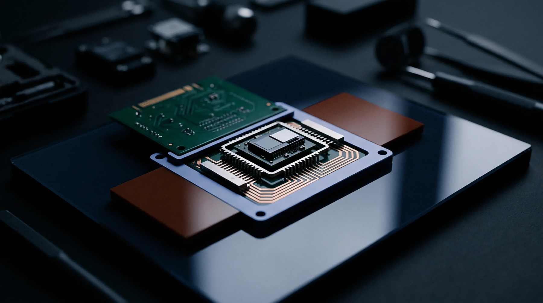
Wafer-level package parasitic inductance variance shifts serial channel return loss and eye margins, requiring strict standoff height controls during assembly.
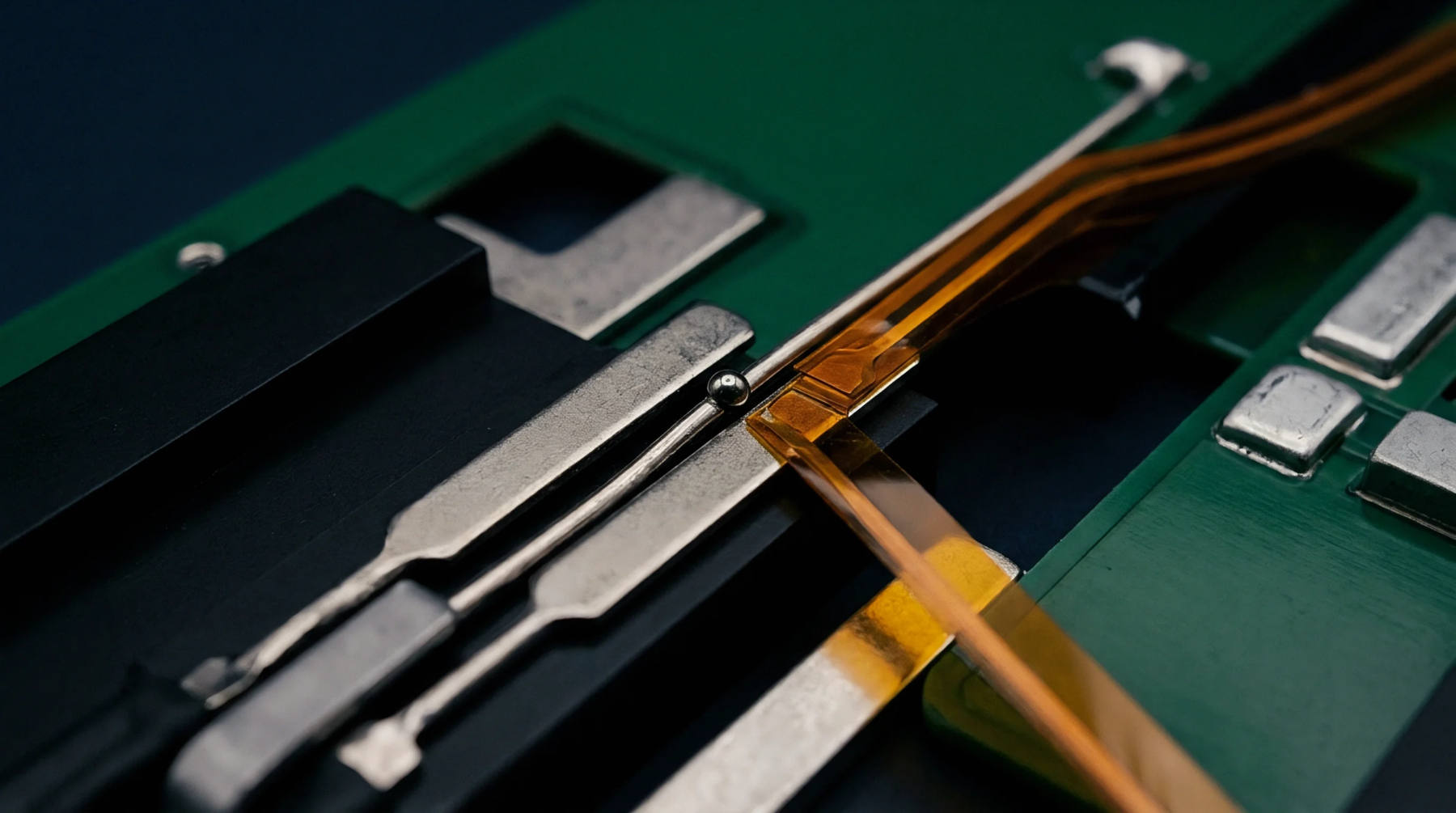
Automated pre-placement socket interrogation of silicon revision registers prevents unannounced wafer steppings from halting high-volume SMT production lines.

Surface mount sensor stepping verification relies on querying internal silicon revision registers over digital buses during automated board testing.
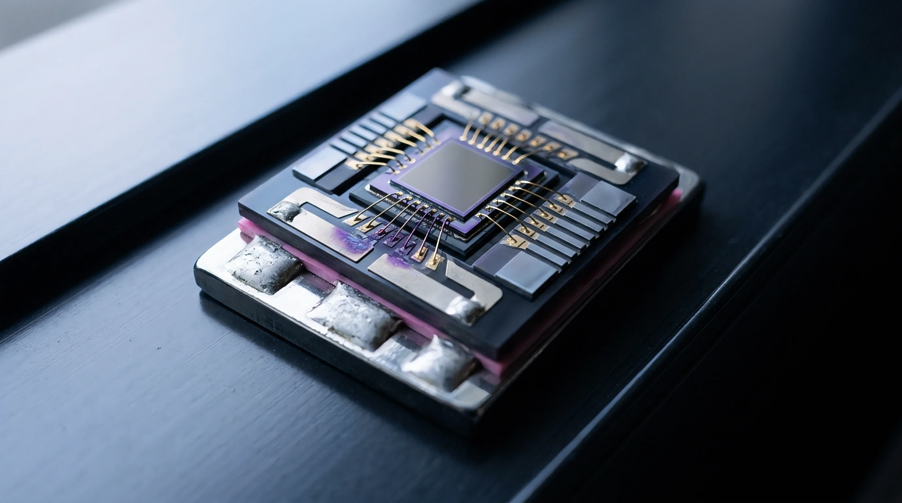
Sensor package selection fixes mechanical strain, driver stability, and break-even volumes before procurement issues purchase orders for alternative parts.

Lead-free solder creep relaxes reflow shear stress at ambient storage temperatures, tilting MEMS anchors and driving uncalibrated zero drift over time.
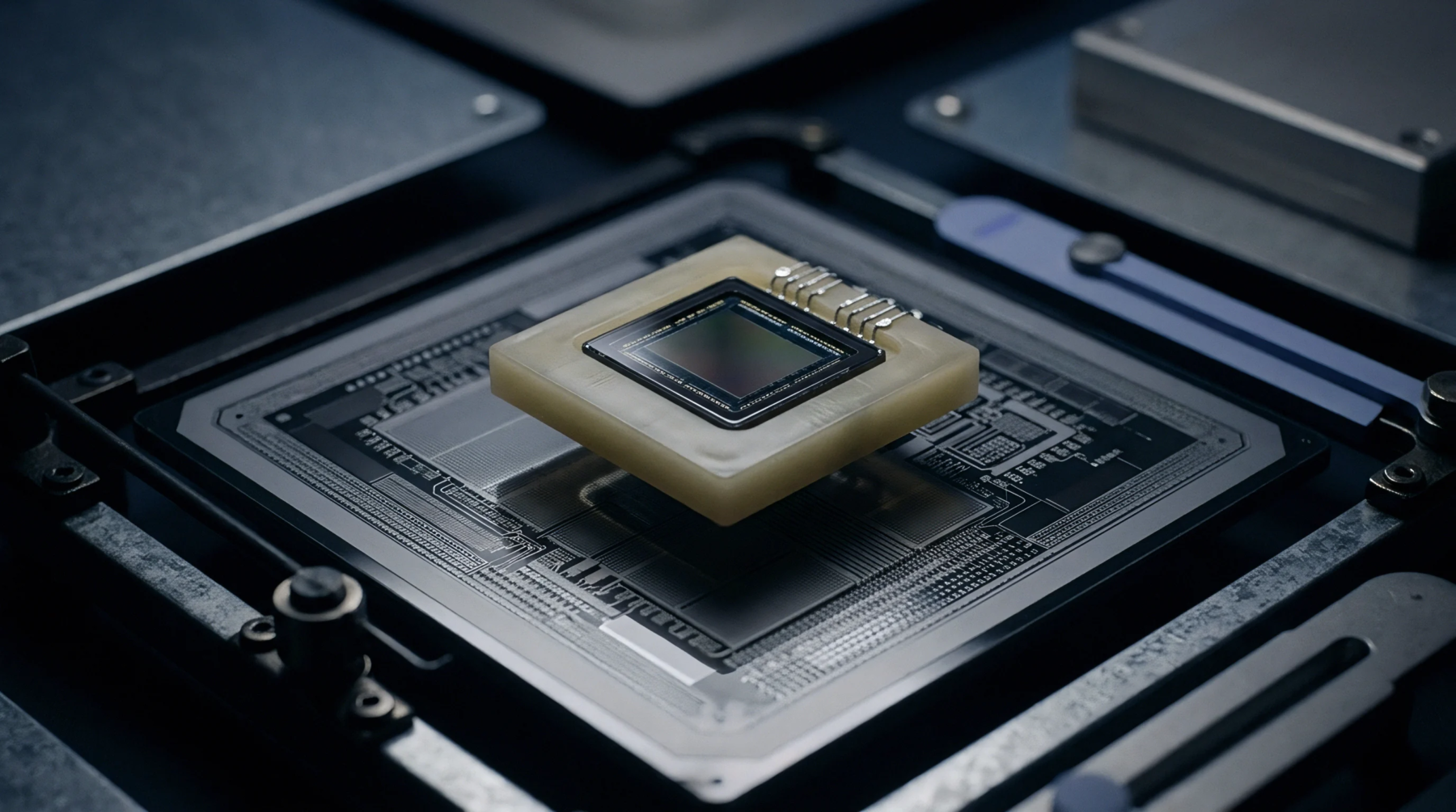
Eliminating protective mold compounds exposes silicon directly to board flexure and solder creep, driving piezoresistive offset shifts across temperature.

Evaluating package parasitics and dynamic reference drive capabilities proves vital to stabilizing dynamic conversion settlement and maximizing AFE accuracy.

Package trace parasitic inductance induces millivolt ground bounce during fast transients, degrading precision reference accuracy without low-loop layout.

Modelling QFN land pattern parasitics balances via inductance, standoff capacitance, and substrate dielectric choices to maintain high-speed interface signal integrity.

Worst case thermal expansion tolerances require arithmetic summation of material displacement and manufacturing variances to preserve solder fillet geometry.
Expertise is a utility, not a secret. sentiention™ publishes its working knowledge as open reference: intelligence layer covering the materials it sources, the markets it enters, and the reference that serves both.