Components Obsolescence Risk Management in Circuit Board Redesign
Mitigate component obsolescence by balancing last-time-buy capital against redesign fees, resolving footprint and bus timing changes before production freezes.


Depletion
Product discontinuance notices arrive with hard calendar deadlines that dictate manufacturing survival. When a semiconductor fabrication facility retires an aging 180-nanometer planar process line, passive and active components vanish from global authorized distribution channels within quarters. Factory lead times on outgoing silicon escalate from 12 weeks to 54 weeks before order books close permanently.
Sourcing teams face an immediate operational divergence between committing capital to end-of-life inventory or triggering an immediate layout revision. A balanced bill of materials prevents factory lines from falling silent.
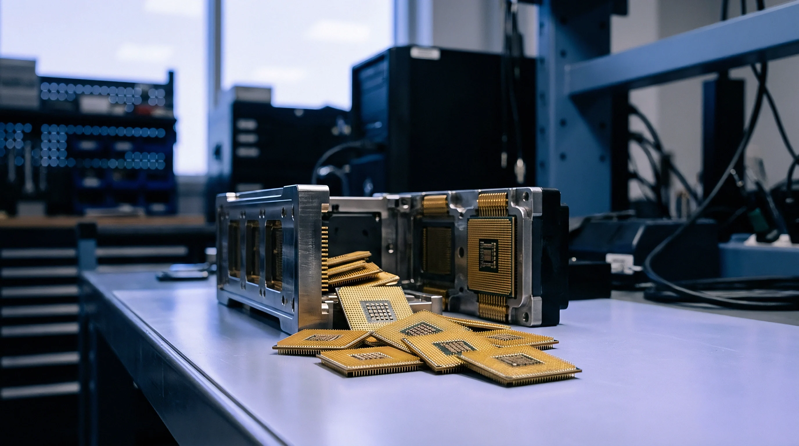
Discontinuation Windows and Last Time Buy Reserves
Official product change notifications define two milestones: the final date to place non-cancelable, non-returnable purchase orders, and the final date factory shipments clear the dock. Between these markers, manufacturing organizations calculate their last time buy buffer based on historical scrap rates, projected field failure replacements, and forecasted unit volumes. Inventory carrying charges accumulate rapidly.
Warehousing sensitive components demands controlled environments meeting moisture sensitivity standards to prevent package delamination during assembly years later.
A factory floor redesign executed twelve months ahead of part extinction preserves existing firmware branches intact.
Capital lockup presents severe financial friction. Purchasing a five-year supply of high-unit-cost mixed-signal microcontrollers strains treasury facilities while exposing the buyer to unmitigated obsolescence risk if end-customer demand contracts. Component degradation represents another physical boundary.
Bare copper leadframes and solder ball alloys oxidize inside dry packs over prolonged storage periods. Solderability testing per J-STD-002 becomes mandatory for lots stored beyond thirty-six months. Moisture barrier bags develop micro-punctures through handling.
Silicon dies remain intact, yet external termination degradation causes line scrap rates to climb during surface mount placement.

Trigger Thresholds between Redesign and Lot Archiving
Engineering modifications carry measurable costs that dictate whether physical redesign beats warehouse stockpiling. A formal assessment balances tooling outlays, regulatory requalification billings, software refactoring cycles, and assembly line retooling against the delivered unit cost of replacement parts. When a component represents low annual turnover, a single last time buy order frequently solves the production requirement.
High-volume industrial assemblies demand immediate schematic migration to current-generation silicon architectures.
- Component spend velocity dictates whether warehouse carry costs exceed total board retooling fees over remaining product service life.
- Active distributor stock levels confirm whether open-market broker sourcing presents an unacceptably high counterfeit infiltration threat.
- Firmware abstraction complexity establishes whether register adjustments consume two engineering weeks or require an entire architectural rewrite.
- Regulatory recertification impact forces early layout freezes whenever industrial safety or wireless approvals require formal laboratory testing.
Suppliers defending sudden line terminations routinely claim that maintenance costs on depreciated wafer stepping machinery make continued production commercially impossible.


Pinout
Silicon revisions inevitably alter package geometry and land footprints. When moving from a legacy packaged sensor to a modern equivalent, engineers rarely secure identical mechanical landing pads. The market trend drives physical outlines from leaded SOIC, TSSOP, and gull-wing packages toward bottom-terminated QFN, DFN, and wafer-level chip scale packaging.
This migration shrinks the occupied circuit board footprint while simultaneously escalating assembly tolerances, thermal sink necessities, and inspection overhead.

Where Does Die Shrinkage Break Pin Compatibility?
Fab migrations shrink the internal silicon surface area, altering bonding pad perimeters and thermal dissipation pathways. Modern silicon geometries place the ground paddle directly underneath the central plastic body rather than distributing thermal return through peripheral pins. Peripheral lead pitch compresses from 1.27 millimeters down to 0.50 millimeters or 0.40 millimeters.
The assembly department adjusts stencil apertures, paste rheology, and optical inspection algorithms to handle these tight clearances.
| Package Type | Lead Pitch (mm) | Footprint Area (mm²) | Coplanarity (mm) | Peak Reflow (°C) |
|---|---|---|---|---|
| SOIC-8 | 1.27 ± 0.05 | 31.0 ± 0.3 | 0.10 max | 240 to 245 |
| TSSOP-14 | 0.65 ± 0.03 | 32.0 ± 0.2 | 0.08 max | 245 to 250 |
| VQFN-16 | 0.50 ± 0.02 | 16.0 ± 0.1 | 0.05 max | 255 to 260 |
| DFN-8 | 0.50 ± 0.02 | 4.0 ± 0.1 | 0.05 max | 255 to 260 |
| WLCSP-12 | 0.40 ± 0.01 | 2.5 ± 0.05 | 0.03 max | 260 max |
Bridging risks increase as pitch decreases. A 0.50-millimeter pitch QFN leaves roughly 0.28 millimeters of copper pad width, allowing a nominal solder mask web of only 0.08 millimeters between adjacent exposed conductors. Board fabricators with standard capability pools struggle to hold solder mask registration within ±0.05 millimeters.
Misregistration exposes adjacent copper edges, inducing solder bridges during mass production reflow passes.
Coplanarity deviations exceeding 0.05 millimeters across a bottom-terminated ground slug yield voiding ratios beyond thirty percent during convection reflow.

Package Translation from Leaded to Bottom Terminated Formats
Transitioning an operational design from gull-wing leads to bottom-terminated pads alters solder joint stress compliance. Leaded components absorb mechanical board flexure through copper alloy leads that flex under mechanical strain. Bottom-terminated components transfer structural board shock and thermal strain directly into solder fillets.
Thermal expansion mismatches between the FR-4 fiberglass substrate and the molded epoxy package concentrate stresses at the perimeter solder joints, inducing low-cycle fatigue cracks over cyclic industrial temperature profiles.
- Intermetallic compound embrittlement occurs along the package boundary when excessive gold plating thickness forms brittle gold-tin phases under standard SAC305 processing.
- Solder joint bridging develops between dense peripheral pads when stencil thickness exceeds 0.10 millimeters on 0.40-millimeter pitch arrays.
- Substrate warpage lift pulls corner terminations off the paste deposit when high-layer-count circuit boards bow inside high-temperature reflow zones.
- Optical inspection blindness prevents automated vision systems from checking pad wetting underneath bottom-terminated components without inline automated X-ray inspection equipment.
Solder mask dams must maintain complete physical separation between adjacent copper pads to prevent paste migration across closely spaced pins.


Copper
Thermal planes and conductive traces govern whether a modified circuit board operates reliably or suffers premature field failure. Replacing an obsolete power regulator or intelligent mixed-signal transmitter changes current path distributions, ground return loops, and heat dissipation balances. Modern components with exposed center pads rely directly on internal board layers to transfer thermal energy away from the silicon die.
When an older board design relied on convection from a wide leadframe, dropping in a compact replacement demands intentional thermal via restructuring.

Thermal Spreader Geometry and Paste Release Dynamics
A continuous central ground pad underneath a component draws heat into inner plane layers. Circuit draftsmen place thermal vias directly into this central land, connecting the surface copper to continuous internal ground planes. Uncapped open vias wick solder away from the component underside, leaving large cavities that isolate the package mechanically and thermally.
Plugging and capping these vias per IPC-4761 Type VII specifications maintains paste volume stability and prevents thermal runaway under full load.
| Surface Finish | Coating Thickness (µm) | Shelf Life (Months) | Thermal Shock Cycles to Fail |
|---|---|---|---|
| ENIG (Ni/Au) | 3.0 to 6.0 Ni / 0.05 to 0.1 Au | 12 to 24 | 1,200 ± 150 |
| OSP (Organic) | 0.2 to 0.5 Organic film | 6 | 950 ± 120 |
| Immersion Silver | 0.12 to 0.40 Ag | 12 | 1,100 ± 110 |
| Immersion Tin | 1.0 to 1.2 Sn | 6 to 12 | 850 ± 90 |
| Thermal shock cycling conditions conducted from -40°C to +125°C with 30-minute dwell times per IPC-SM-785. | |||
Substrate finish alters joint longevity. Electroless nickel immersion gold provides a flat contact surface suited for fine-pitch parts, yet nickel phosphorus corrosion during plating introduces hyper-corrosion black pad defects. Organic solderability preservatives degrade under multiple thermal reflow cycles, limiting assembly flexibility on double-sided circuit cards.
Solder joint shear fatigue accelerates when localized dielectric thickness changes alter thermal expansion differentials between package and substrate.

Breakout Routing Densities across Substrate Revisions
Signal line geometries contract when components compress their contact grids. Standard trace and space widths of 0.127 millimeters suffice for 0.80-millimeter pitch parts. Moving to modern 0.40-millimeter pitch packaging demands 0.075-millimeter or 0.065-millimeter trace geometries.
Circuit board fabricators charge premium manufacturing additions for trace features under 0.100 millimeters due to etching yield losses. Impedance control tolerances drift wider when etching thin copper weights across large panel formats. Designers who omit these manufacturing constraints face unresolvable board yield fallout during initial production runs.
Ignoring copper layer rebalancing causes uneven panel bow that tears internal blind vias during secondary soldering passes.


Bus
Hardware compatibility extends across the physical trace into digital signaling transactions. Swapping an obsolete digital sensor or peripheral bridge device introduces interface protocol discrepancies. Two components sharing the same generic I2C or SPI interface descriptor often display radically divergent electrical behavior, timing margins, and internal register memory arrangements.
Firmware engineers discover these discrepancies when the replacement component fails to acknowledge basic read commands during cold hardware bring-up.

Will Alternate Transceivers Tolerate Mismatched Capacitive Loading?
Electrical signal rise times govern digital communication reliability. The standard I2C specification fixes maximum bus capacitance at 400 picofarads for fast-mode operation running at 400 kilohertz. Legacy devices incorporate weak internal pull-up structures or tolerate high input pin capacitances.
Modern replacement parts present differing input gate capacitances, altering signal edge rise times. Sizing external pull-up resistors too low over-saturates the driver sinking current, exceeding the open-drain low-level output voltage limit of 0.4 volts. Sizing resistors too high produces sluggish rising edges that fail minimum setup time requirements.
A systematic evaluation checklist resolves interface timing and operational risks:
- Bus line pull-up sizing confirms edge transition times fall within specified standard limits without violating output driver current sink maximums.
- Clock stretching accommodation prevents microcontroller peripherals from hanging when a slower successor component holds the serial clock line low.
- Address line strap flexibility avoids hardware collisions with hard-coded peripherals sharing the same electrical circuit lines.
- Serial peripheral clock phase settings match host controller SPI data latches to incoming device propagation delays over line temperature extremes.
- Power rail voltage tolerance matches legacy 5.0-volt operational domains with contemporary 3.3-volt or 1.8-volt digital input thresholds without line ringing.

Command Dialect Shifts and Register Map Divergence
Silicon manufacturers rarely maintain backward register compatibility across separate die generations. An obsolete sensor that exported sixteen-bit signed integer values across two sequential read operations often cedes ground to a successor device that packs measurements into twenty-four-bit fixed-point formats with interspersed status flags. Internal state machines require unique initialization handshakes, clock configuration sequences, and interrupt clear routines.
Microcontroller software drivers demand thorough refactoring, expanding verification testing schedules by multiple engineering weeks.
A designer facing mismatched silicon updates must determine whether host driver abstraction layers can isolate timing variations without exhausting microsecond interrupt budgets.


Settlement
Commercial liabilities and cost allocations define the final viability of a circuit board revision program. Engineering hours, stencil tooling, prototype iterations, and testing chamber bookings accumulate rapidly during a component replacement effort. Sourcing specialists evaluate piece-part savings against these fixed development outlays to establish precise financial break-even volumes.
Sourcing teams also monitor distributor price structures, minimum order thresholds, and factory cancellation terms to shield operations from supply shocks.

Direct Sourcing Variance and Minimum Order Penalties
Component piece prices fluctuate dramatically across package configurations. Bare silicon sold as wafer-level chip scale packages commands low unit costs at extreme production volumes, yet carries strict minimum order quantities reaching tens of thousands of units per order code. Tape-and-reel packaging formats impose minimum reel quantities that trap capital when building low-volume industrial equipment.
Standard distributors charge premiums of thirty to eighty percent when breaking reels into cut-tape strips for pre-production prototype runs.
| Expense Category | Drop-in Equivalent ($) | Footprint Redesign ($) | Architectural Overhaul ($) |
|---|---|---|---|
| Schematic and Layout Hours | 500 to 1,200 | 3,500 to 8,000 | 12,000 to 25,000 |
| Firmware Driver Refactoring | 0 to 800 | 2,000 to 6,000 | 8,000 to 20,000 |
| PCB Tooling and Stencils | 0 | 800 to 2,500 | 1,500 to 4,000 |
| EMC and Environmental Testing | 0 to 1,500 | 4,000 to 12,000 | 10,000 to 30,000 |
| Total Upfront Commitment | 500 to 3,500 | 10,300 to 28,500 | 31,500 to 79,000 |
Upfront engineering fees establish the break-even production threshold. Amortizing twenty-eight thousand dollars of design expenses across a manufacturing run of five thousand units adds five dollars and sixty cents to each delivered board. Sourcing professionals balance this amortization penalty against the unit purchase price differential between obsolete legacy parts secured through independent broker stock and direct-from-foundry modern silicon alternatives.
Incorporation of standard J-STD-048 notification windows binds the semiconductor distributor to one hundred and eighty days between discontinuance notice and final bookable order date.

Requalification Expenses across Industrial Compliance Regimes
Regulated markets impose strict recertification burdens when circuit components change. Medical products certified under IEC 60601-1 or industrial functional safety assemblies governed by IEC 61508 treat mixed-signal component changes as major product alterations. Engineering teams conduct electromagnetic compatibility scans, electrostatic discharge susceptibility sweeps, and climatic chamber stress testing to assemble an updated compliance dossier.
These laboratory testing fees exceed layout engineering expenses, cementing the total redesign budget.
Standard procurement agreements stipulate that non-cancelable commitments apply immediately upon receipt of formal factory production scheduling confirmations.