Bandgap Reference Output Shift under Solder Reflow Thermal Stress
Reflow thermal stress alters bandgap reference outputs by up to 1500 ppm via piezoresistive die strain, demanding compliant packages, bakes, or in-system trim.

Offset
Precision analog circuits rely on predictable bandgap potentials, but reflow soldering routinely introduces permanent voltage shifts larger than datasheet initial accuracy limits. When a factory trim guarantees 0.05 percent error, it measures a bare, unmounted die or a part sitting on a tape reel. Once that component passes through lead-free assembly temperatures peaking between 245°C and 260°C, thermal stress drives through the plastic mold compound, straining the silicon lattice and shifting the core voltage enough to degrade high-resolution measurements.
Depending on the package and board geometry, this voltage shift typically lands between 100 parts per million and more than 1500 parts per million. In a 16-bit analog-to-digital converter signal chain with a 2.500 V span, one least significant bit is just 38 microvolts. A reflow shift of 0.08 percent swings the baseline by 2.000 millivolts ~ wiping out over 52 quantization steps before the converter samples anything.
Unexplained calibration failures at end-of-line testing often trace straight back to the thermal profile in the reflow oven.
Peak reflow exposure at 260°C shifts standard plastic-packaged bandgap outputs by up to 1200 parts per million under standard convection profiles.

Piezoresistive Coupling inside Silicon References
Mechanical stress alters carrier mobility and bandgap structure in crystalline semiconductors. In a standard Brokaw cell or proportional-to-absolute-temperature circuit, bipolar transistors run at matched current densities to extract thermal voltage. Because silicon has strong piezoresistive coefficients along its Miller indices, longitudinal and transverse compressive stresses shift base-emitter saturation currents unevenly across asymmetric layouts, changing the differential base-emitter voltage directly.
When stress is distributed unevenly across the die surface, the theoretical cancellation of temperature coefficients falls apart. The bandgap core adds a complementary-to-absolute-temperature base-emitter voltage to a scaled positive-temperature-coefficient differential voltage. If post-reflow stress skews the junction saturation currents, that programmed balance breaks down, accelerating drift across operating temperatures and degrading both zero-scale accuracy and thermal slope.
Factory Calibration Erosion across Package Families
Wafer-level laser trimming and electrically programmable fuses tune thin-film resistor networks while the silicon rests in mechanical equilibrium at room temperature. Surface-mount soldering shatters that balance. Differential thermal expansion across the package body, leadframe, and die attach subjects the chip to severe thermal shock, and as the molding compound shrinks during cooldown, it clamps the die in a permanent compressive vice.
How much of that shock reaches the silicon depends on leadframe compliance and encapsulation thickness. Smaller packages bring the die closer to the PCB surface, which amplifies the thermal strain conducted through the solder joints.
Ignoring post-assembly reference shifts guarantees calibration failures once boards reach functional testing.

Joint
The solder joint is the mechanical bridge that transfers thermal expansion mismatch from the circuit board into the die paddle. Most lead-free production relies on SAC305, which solidifies at 217°C rather than the 183°C of eutectic tin-lead. That higher melting point forces peak oven zones up to 245°C or 260°C, widening the temperature drop during cooldown.
Once the molten alloy freezes, it locks the board laminate and component body together in an inelastic bond.
Copper pads, bulk solder, and component terminations all carry different coefficients of thermal expansion. FR-4 expands in-plane at 14 to 17 parts per million per Kelvin and copper traces at 16.5 parts per million per Kelvin, whereas silicon expands at just 2.6 parts per million per Kelvin. As the board cools from liquidus to room temperature, the substrate contracts roughly six times faster than the silicon die, driving shear directly into leadless footprints.
| Package Configuration | Leadframe Material | Typical Die Shift (ppm) | Maximum Die Shift (ppm) | Board Flex Sensitivity (ppm/mm) |
|---|---|---|---|---|
| SOIC-8 | Alloy 42 | 120 | 350 | 45 |
| SOIC-8 | Copper CDA 194 | 220 | 580 | 85 |
| MSOP-8 | Copper CDA 194 | 380 | 850 | 140 |
| SOT-23-5 | Copper CDA 194 | 450 | 1100 | 195 |
| DFN-8 (3×3 mm) | Copper Exposed Pad | 650 | 1450 | 310 |
| WLCSP-6 (Wafer-Level) | Silicon Direct | 900 | 2200 | 520 |

Solder Alloy Solidification and Thermal Profiles
How long a board remains above liquidus dictates how coarse the solder microstructure becomes. Spending too much time above 217°C produces thick, brittle copper-tin intermetallic layers along the pad boundary. Conversely, rapid cooling at 3°C to 4°C per second creates fine dendrites that raise joint yield strength, transmitting higher stresses into the package body as uneven cooling locks in residual shear.
Ramp rates also set up thermal gradients across the board assembly. If an internal ground plane beneath a reference pulls heat away faster than neighboring signal traces, solder on one side of the package solidifies first. This uneven freeze twists the leadframe, tilting the die and straining thin-film resistors on the chip face.

Package Architecture and Mechanical Transfer Chains
Gull-wing leads on SOIC packages flex under load, absorbing board shear before it reaches the mold compound. Quad-flat no-lead devices and wafer-level chip-scale packages offer no such compliance; their short, rigid joints transfer board contraction straight into the silicon. On DFN packages, the central exposed thermal pad forms a large solder joint directly beneath the sensitive analog core, locking the die paddle to the PCB copper.
- Intermetallic Growth builds brittle copper-tin boundary layers that pass mechanical shock straight to the leadframe.
- Substrate CTE Mismatch sets up lateral shear because FR-4 contracts six times faster than silicon during post-reflow cooldown.
- Exposed Die Paddle Soldering anchors the active core directly to the board through a stiff thermal joint, coupling board warpage into the circuit.
- Solder Fillet Asymmetry exerts twisting moments on the package whenever paste volume varies across opposing pads.
IPC-A-610 Class 3 heel fillet criteria dictate full wetting heights that inadvertently increase the mechanical stiffness of gull-wing leads.
Component factory testing guarantees initial baseline accuracy, while downstream assembly line profiles remain the responsibility of the system integrator.

Relaxation
Mechanical equilibrium inside a surface-mount assembly takes hundreds of hours to settle after reflow. Epoxy novolac mold compounds creep under the compressive stress locked in during cooldown. Voltage outputs show their worst departure from factory trim the moment boards leave the cooling zone.
As polymer chains gradually relax, residual shear dissipates and the silicon lattice settles back toward its untensioned state.
This recovery follows a logarithmic decay curve. Roughly 50 percent of recoverable drift clears within the first 48 to 72 hours at 25°C. Full mechanical settling takes between 168 and 1000 hours of unpowered dwell, governed by package size and filler content. Moisture ingress complicates matters further: as the epoxy absorbs ambient humidity, the matrix swells, creating secondary stresses that either counteract or worsen the initial thermal shift.
| Stabilization Schedule | Dwell Environment | Throughput Impact | Average Stress Relief (%) | Residual Shift (ppm) |
|---|---|---|---|---|
| Ambient Dwell (24 Hours) | 25°C, 40% RH | Minor buffer holding | 35 | 450 |
| Ambient Dwell (168 Hours) | 25°C, 40% RH | High inventory backlog | 60 | 280 |
| Accelerated Thermal Bake | 125°C, Dry Air, 24 Hours | Oven batch processing | 85 | 110 |
| Extended Thermal Bake | 125°C, Dry Air, 48 Hours | Extended batch time | 92 | 65 |
| High-Temp Bake with Pre-Bake | 150°C, Dry Air, 12 Hours | Thermal stress risk | 88 | 90 |

Viscoelastic Settling of Epoxy Molding Compounds
Molding compounds combine an organic resin matrix with fused silica spheres that bring the package CTE closer to copper. Below the glass transition temperature ~ typically 140°C to 160°C ~ the compound acts as a glassy solid with an elastic modulus above 20 gigapascals. When reflow temperatures cross that threshold, the resin softens and expands rapidly.
As the board cools back through the transition zone, non-equilibrium volume contractions freeze in place, unwinding only through slow molecular rearrangement.
Silicon piezoresistance mirrors this relaxation. As the surrounding mold compound eases its grip, internal transistor bias currents shift back toward their original values. Because plastic deformation in the solder alloy and intermetallic structures do not anneal at room temperature, that recovery remains incomplete, leaving a permanent residual offset.
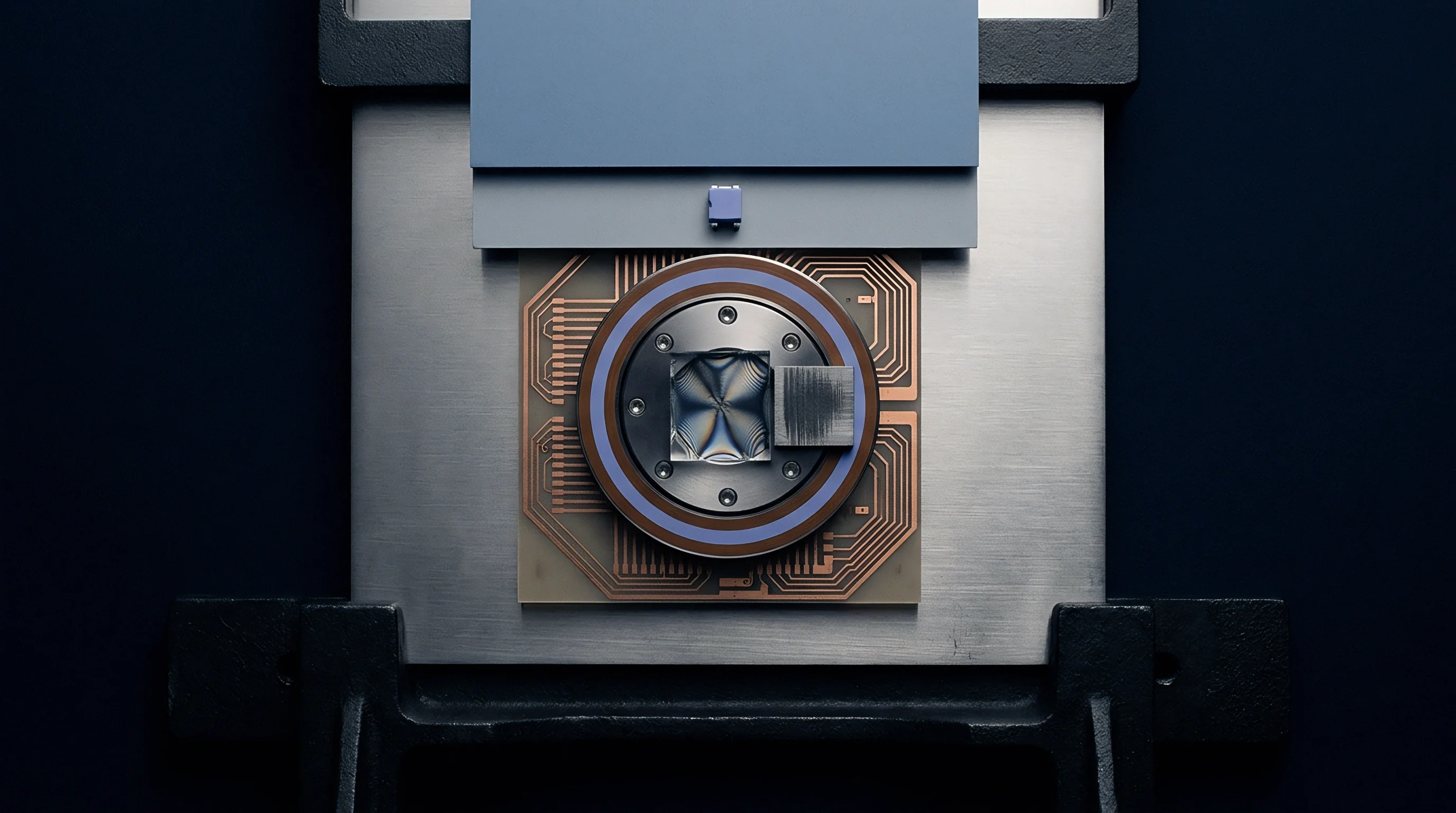
Thermal Annealing Schedules for Board Assemblies
Production schedules rarely allow boards to sit in holding buffers for seven days before final test and calibration. Controlled baking condenses that viscoelastic relaxation from weeks into hours. Running assembled boards through a 24-hour bake at 125°C accelerates polymer relaxation, shedding trapped mold stress while annealing solder joint microstructures.
Consider a production run of precision data acquisition boards built with an MSOP-8 packaged 2.500 V reference rated to an initial 0.05 percent (1250 microvolt) tolerance. Probing the parts directly after SAC305 reflow shows an average negative shift of 750 ppm (1875 microvolts), failing end-of-line limits. Adding a 24-hour bake at 125°C followed by a 4-hour ambient dwell recovers 85 percent of that shift, leaving a permanent offset of just 112 ppm (280 microvolts) and keeping the design within its resolution budget.
Whether prolonged thermal annealing prevents secondary drift during automotive field deployment across operating extremes remains an open question.


Placement
Board layout largely dictates how much mechanical stress reaches a soldered reference. Printed circuit boards behave like diaphragms, flexing under thermal cycling, vibration, and chassis mounting forces. Dropping a sensitive bandgap reference into the center of a large, unsupported board exposes the die to maximum deflection.
Aligning the package leads parallel to the primary bending axis helps minimize tensile strain across the silicon face.
Copper distribution through the stack-up also determines local board flatness. Asymmetrical copper layers encourage localized warpage as the board cools through the solder liquidus zone. Flooding solid copper under a reference on the surface layer while leaving adjacent inner layers empty causes distinct convex bowing.
Balancing copper weight across layers prevents that localized distortion.
Placing sensitive analog references along the neutral axis of the assembly isolates the silicon die from external board flexure.
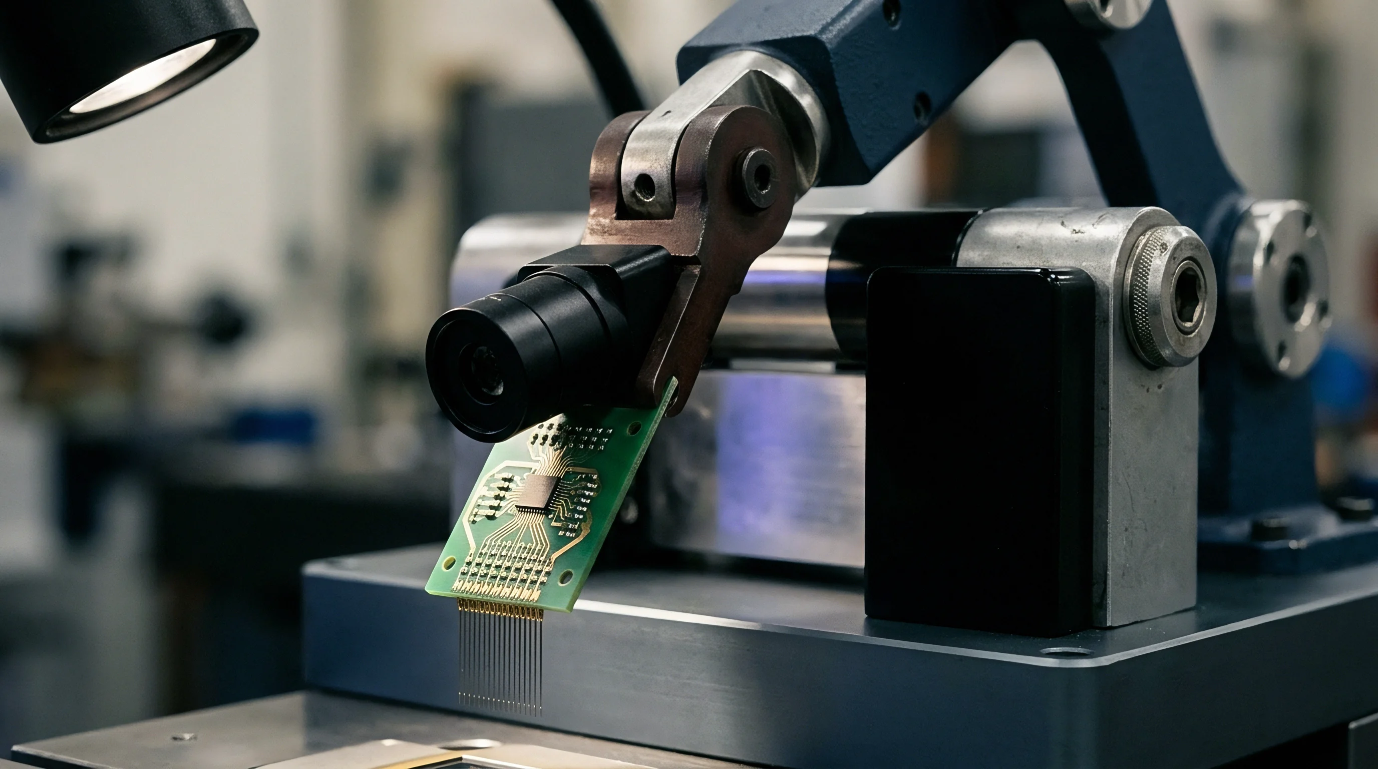
Crystallographic Orientation and PCB Bending Axes
Standard silicon wafers are cut along crystallographic planes, with active structures aligned to the wafer flat or notch. Because longitudinal piezoresistive sensitivity peaks along this axis, aligning the package length with the longer dimension of the panel limits the curvature transferred during handling and assembly.
Mismatched pad sizes generate rotational torque during reflow. If a trace tied to one terminal is markedly wider than the trace on the opposite pin, differences in thermal mass cause the solder joints to freeze at different times. Surface tension pulls the component off-axis, locking asymmetric mechanical stress into the package frame.
- Position the reference IC away from heat sources like power inductors and linear regulators to prevent local thermal gradients.
- Maintain a minimum clearance of 25 millimeters from chassis standoffs to shield the package from screw torque.
- Orient the package length parallel to the shortest edge of the circuit assembly to lower flexural displacement during board bending.
- Ensure symmetrical trace geometries on all terminal pins to balance surface tension forces as the solder freezes.
- Incorporate perimeter routing relief slots around precision analog sections to decouple the reference from board warpage.
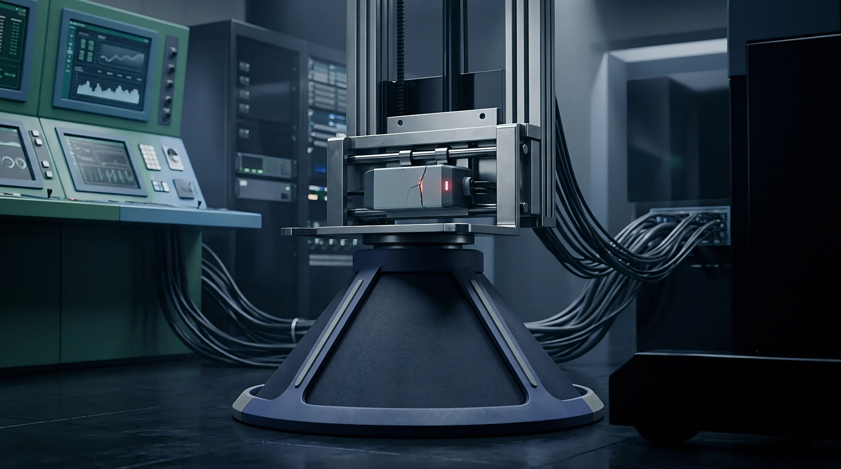
Keepout Rules near Fasteners and Depaneling Cuts
Depaneling subjects assemblies to sharp shock pulses and board deflection. V-scoring wheels and snap-off breakout transmit heavy shear waves through the laminate; placing a reference within 10 millimeters of a score line can trigger voltage shifts that dwarf the reflow offset. Routing tabs with a milling spindle cuts down that shock, though residual distortion near the cut remains.
Mounting fasteners create similar problems. Any reference sitting inside the strain shadow of a chassis screw experiences direct voltage offsets when torque is applied, as substrate flex couples straight into the silicon core.
Treating precision voltage references like standard digital ICs in PCB layout almost guarantees baseline instability across production hardware.

Expense
Part selection balances bill-of-materials cost against the production overhead required to tame shifted reference voltages. Silicon bandgap architectures are packaged across a steep price ladder. SOT-23 variants sit at the bottom at 0.45 dollars in volume, but remain vulnerable to reflow shift and board flexure.
Moving up to an SOIC-8 package raises unit cost to 1.15 dollars while adding compliant gull-wing leads that absorb solder strain.
At the top of the ladder sit hermetic ceramic packages like LCC-8 envelopes, running between 12.00 and 18.00 dollars each. Because gold-tin or silver-copper eutectic alloys seal the cavity without placing polymer mold compound in contact with the die, ceramic packages eliminate epoxy shrinkage stress entirely.
| Variant Form Factor | Unit Cost @ 10k (USD) | Board Space (mm²) | Post-Reflow Shift (ppm) | Downstream Mitigation Required |
|---|---|---|---|---|
| WLCSP-6 | 0.38 | 2.1 | 1800 | Mandatory post-assembly system calibration |
| SOT-23-5 | 0.48 | 9.0 | 950 | Thermal anneal bake or digital trim |
| DFN-8 (3×3 mm) | 0.82 | 9.0 | 1200 | Perimeter PCB routing slots and bake |
| MSOP-8 | 0.75 | 15.0 | 700 | Standard production hold or anneal |
| SOIC-8 | 1.25 | 31.0 | 320 | Minimal mitigation for 12-bit chains |
| Ceramic LCC-8 | 14.50 | 25.0 | 45 | None; direct solder mounting permissible |

The Variant Price Spread from SOT to Hermetic
Specifying an inexpensive SOT-23 reference often shifts financial burden down onto the factory floor. A 24-hour annealing cycle at 125°C ties up industrial ovens, inflates work-in-progress inventory, and draws steady electrical power. The break-even point between packaging and processing depends heavily on production volume and test floor capabilities.
On a line running 100,000 boards a year, tying up 24 hours of batch oven capacity costs roughly 0.18 dollars per board in equipment depreciation and operator time. Adding a digital calibration step consumes 4 to 8 seconds of automatic test socket time, billed at about 0.05 dollars per second on a typical mixed-signal tester. Spending more upfront on an SOIC-8 package often pays for itself by eliminating bake cycles and shortening test sequences.

In-System Trim against High Grade Packaging
Mixed-signal controllers provide a way to work around expensive packaging through software. Designers can store calibration constants in an EEPROM lookup table or adjust a non-volatile digital potentiometer during final functional test. An external reference standard probes the board via dedicated test pads to measure the actual post-reflow output voltage, allowing the host microcontroller to compute the error against nominal and write a permanent correction factor to flash.
- Hardware Expense stays low because digital calibration absorbs physical package drift in cheap plastic parts.
- Firmware Complexity rises to handle non-volatile calibration registers and initialization routines on boot.
- Test Floor Overhead increases because the fixture requires thermally stabilized external voltage standards.
- Field Service Liabilities arise if non-volatile memory drops calibration coefficients during a brownout or power cut.
Procurement contracts for precision references routinely reference J-STD-020 reflow profiles, releasing the vendor from output tolerance specifications once package body temperatures exceed published assembly limits.