Piezoresistive Pressure Sensor Packaging Baseline Properties
Selecting piezoresistive pressure packaging requires matching media isolation, land pattern strain limits, and bus interfaces to control unit cost.

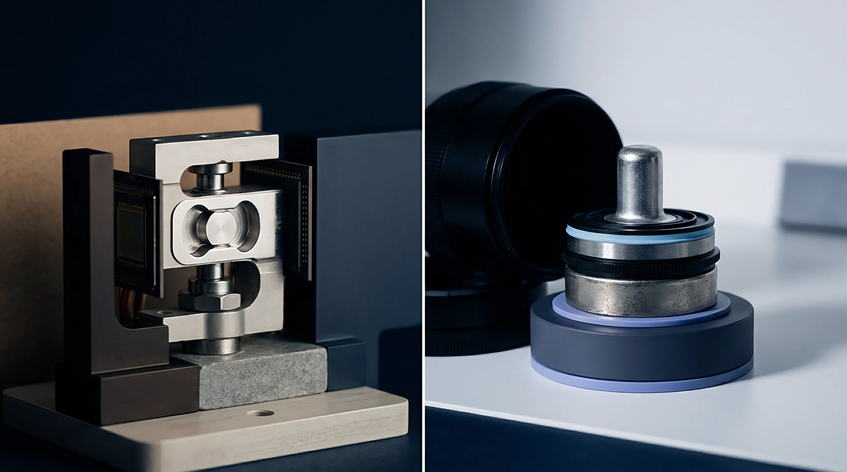
Vent

Media Access Architecture and Cavity Isolation
Transferring pressure to a silicon piezoresistive element requires a direct path from the environment to the diaphragm face. Micromachined silicon dies sense pressure as a thin etched membrane containing piezoresistors flexes under load. This deformation alters electrical resistance predictably, but direct contact with the fluid medium leaves unsealed die cavities, wire bonds, and metal traces vulnerable to moisture, vapors, and debris.
Packaging must therefore adapt the port’s internal boundary layer depending on whether the media is a clean gas or a harsh liquid.
Gaseous pressure ports rely on open cavity molded plastic structures or metal headers. Top-port Land Grid Array (LGA) and Quad Flat No-Lead (QFN) configurations place a stamped lid with a port hole directly over the silicon die. Atmospheric reference paths for gauge pressure measurements pass through the bottom of the substrate or through an unsealed top port.
Absolute pressure references enclose a vacuum cavity behind the diaphragm during anodic or glass-frit wafer bonding. The cavity shape establishes the dead volume, which directly influences response dynamics and fluid retention under condensation cycles.
Fluorosilicone gel fill buffers the silicon diaphragm against liquid contact while transferring hydraulic pressure without attenuation across operating temperatures.
Aggressive liquids require an isolating gel layer over the sensing surface. Siloxane-based or fluorosilicone compounds fill the upper cavity of Small Outline Integrated Circuit (SOIC) packages and custom modules, balancing chemical inertness against mechanical stiffness. Stiffer gels with high Shore hardness transfer package stresses directly to the diaphragm edges, creating temperature-dependent offset errors.
Conversely, low-viscosity gels maintain fast dynamic response but tend to bubble and degas under vacuum. As operating temperatures shift, the volumetric expansion of the gel pulls or pushes on the surface, moving the zero-point voltage baseline.

Atmospheric Reference Routing and Port Mechanics
Gauge and differential sensors need a clear reference path to the back of the die. On surface-mount designs, this secondary path usually routes through a center hole in the circuit board. Solder mask, flux, or conformal coating can easily clog this sub-millimeter hole during reflow or assembly.
Blocking the reference port converts a gauge sensor into an accidental sealed-cavity system, where ambient temperature shifts alter internal pressure and skew readings.
Dual-port modules avoid board-level contamination by placing the reference channel inside a dedicated barbed or threaded fitting. The geometry of these ports dictates hose retention and seal integrity. Parameters like barb pitch, barb angle, and nozzle concentricity determine whether tubing stays leak-tight during high-pressure transients.
Machined brass and injection-molded polyphthalamide (PPA) housings hold tolerances within plus or minus 0.05 millimeters across production runs.
Corrosive fluids call for total isolation between the process media and the internal packaging. In these environments, stainless steel diaphragms with internal oil fills isolate the silicon piezoresistive die. Welded 316L stainless steel headers housing oil-filled cavities increase mechanical envelope size and unit price.
Dropping an unisolated, gel-filled top-port package into an environment exposed to acidic condensate leads to corroded bond pads, delaminated wire bonds, and complete sensor output failure within weeks of field deployment.


Land
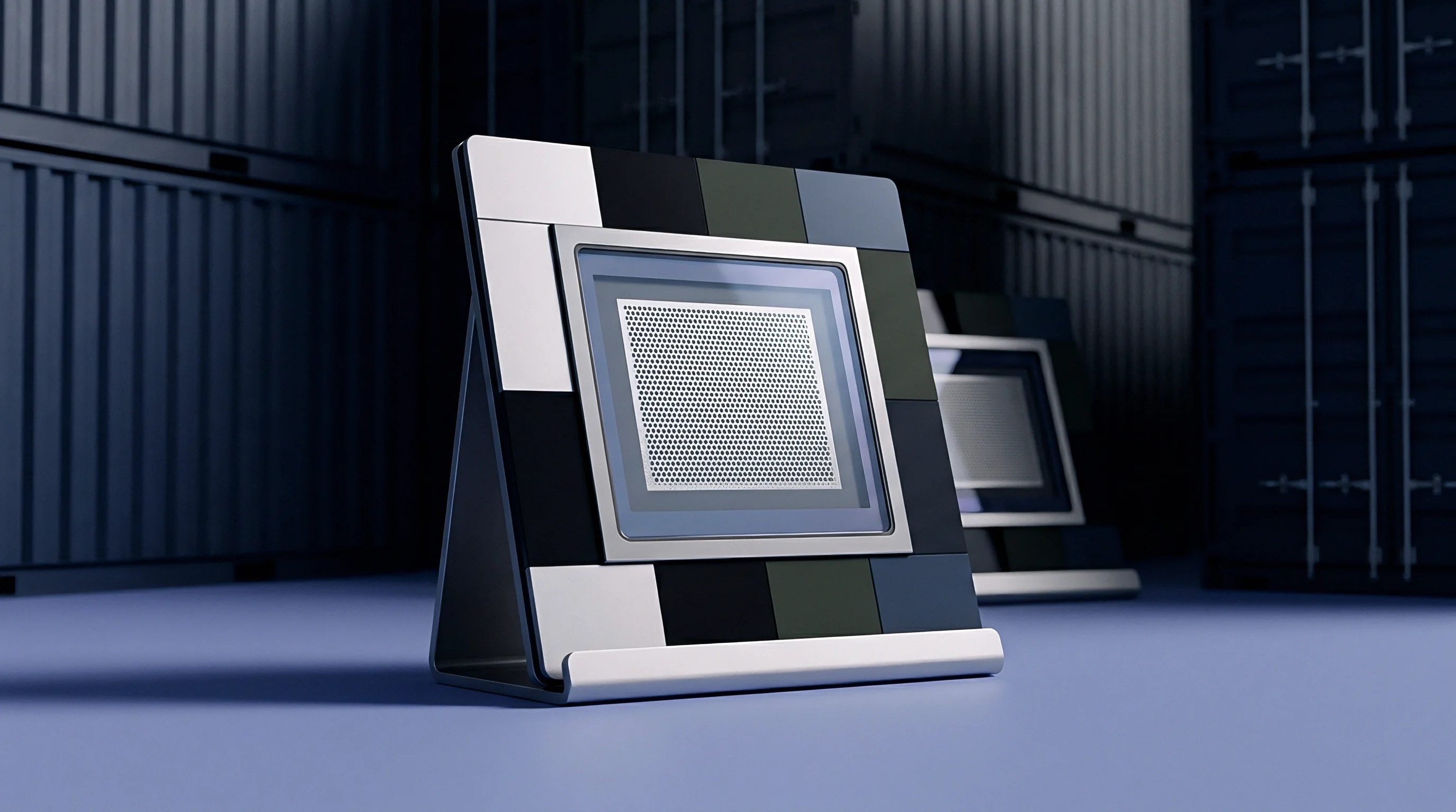
Surface Mount Packaging Mechanics and Substrate Stresses
Circuit boards expand and contract far more than single-crystal silicon. Standard FR-4 substrates have a thermal coefficient of expansion between 14 and 17 parts per million per degree Celsius, whereas silicon stays near 2.6 parts per million per degree Celsius. Direct soldering subjects the package to shear forces across the solder joints during temperature swings.
These stresses pass through the leadframe or pads into the die-attach adhesive, distorting the silicon lattice and shifting the zero-point output.
Package geometry sets how much board stress reaches the die. Standard Small Outline Package (SOP) designs use gull-wing leadframes to absorb movement through compliant metal legs. By contrast, Quad Flat No-Lead (QFN) and Land Grid Array (LGA) packages sit close to the board on rigid bottom pads, increasing mechanical coupling to the piezoresistive element.
Using thicker, low-modulus die-attach adhesives helps cushion the expansion mismatch, but can introduce long-term mechanical creep under sustained pressure loads.
| Package Format | Nominal Footprint (mm) | Height (mm) | Board Stress Coupling | Media Compatibility | Typical MSL |
|---|---|---|---|---|---|
| LGA-8 Top Port | 3.00 x 3.00 ±0.10 | 0.90 ±0.05 | High | Clean Dry Air | 1 |
| QFN-10 Dual Port | 4.00 x 4.00 ±0.15 | 1.60 ±0.10 | Moderate-High | Non-corrosive Gases | 3 |
| SOIC-8 Gel Filled | 4.90 x 3.90 ±0.15 | 1.75 ±0.10 | Low-Moderate | Liquids / Humidity | 3 |
| Stainless Steel Module | 19.00 Diameter ±0.20 | 12.50 ±0.30 | Negligible | Aggressive Liquids | 1 |

Footprint Layout and Reflow Soldering Parameters
Stencil aperture design controls solder volume and joint geometry beneath surface-mount sensors. Too much solder on central pads or corner leads causes non-uniform tilting across the package body. This tilt imposes asymmetric mechanical stress across the piezoresistive bridge, splitting the differential output voltage even at zero applied pressure.
Stencils for bottom-terminated sensors typically use segmented window-pane patterns that limit solder coverage to between 50 and 65 percent of the metal pad area.
J-STD-020 guidelines cap peak reflow body temperature at 260 degrees Celsius to prevent thermal degradation of internal gel fills and die bonds.
The thermal profile during reflow dictates how much residual stress stays locked in the assembly after cooling. Cooling faster than 3 degrees Celsius per second solidifies SAC3005 or SAC305 lead-free solders too quickly, trapping compressive stress that causes large post-assembly offset errors. Holding the ramp-down rate between 1.5 and 2.0 degrees Celsius per second gives the solder matrix time to relax and stabilizes the zero-pressure baseline output.
Trace routing near the land pattern alters local board stiffness. Heavy copper planes or clusters of plated through-holes next to sensor pads create rigid spots on the board. As the board undergoes thermal cycling, uneven copper distribution twists the package body.
Machine layout guidelines mandate symmetric trace entry on all pads and at least 3.0 millimeters of clearance between the package edge and any board cutouts, mounting screws, or press-fit connectors.
- Solder Joint Fatigue occurs when thermal cycling generates microscopic cracks across rigid LGA corner pads, progressively shifting bridge resistance over operational lifespans.
- Substrate Warpage transfers flexural strain through the die-attach epoxy into the silicon piezoresistors when mounting torque is applied to the board.
- Gel Delamination breaks the protective seal between cavity walls and siloxane fill when thermal reflow ramp rates are too high.
- Atmospheric Port Occlusion results from liquid solder flux entering reference openings located on the underside of surface-mount substrates.
Fitting these stress-sensitive piezoresistive footprints into dense board layouts requires balancing tight component spacing against strict mechanical isolation zones.


Wire

Signal Conditioning Architectures and Interface Physics
Unconditioned piezoresistive bridges output small differential voltages, typically spanning 10 to 20 millivolts per volt of excitation full-scale. Packaging an Application-Specific Integrated Circuit (ASIC) alongside the sensor die inside a multi-chip package (MCP) amplifies these signals, runs digital temperature compensation, and delivers a calibrated output. Inter-die wire bonds connect the analog bridge lines directly to high-impedance instrumentation amplifier inputs on the conditioning chip.
Analog ratiometric signals represent the traditional interface style for automotive and industrial monitoring systems. An analog voltage output scales linearly with supply voltage, outputting 0.5 to 4.5 volts across a nominal 5.0-volt supply rail. External Analog-to-Digital Converters (ADCs) in host microcontrollers digitize these values relative to the shared supply reference.
Long cable runs pick up electromagnetic noise and degrade higher-frequency signals, so maintaining signal-to-noise ratios above 60 decibels requires precise filtering networks at the receiving end.
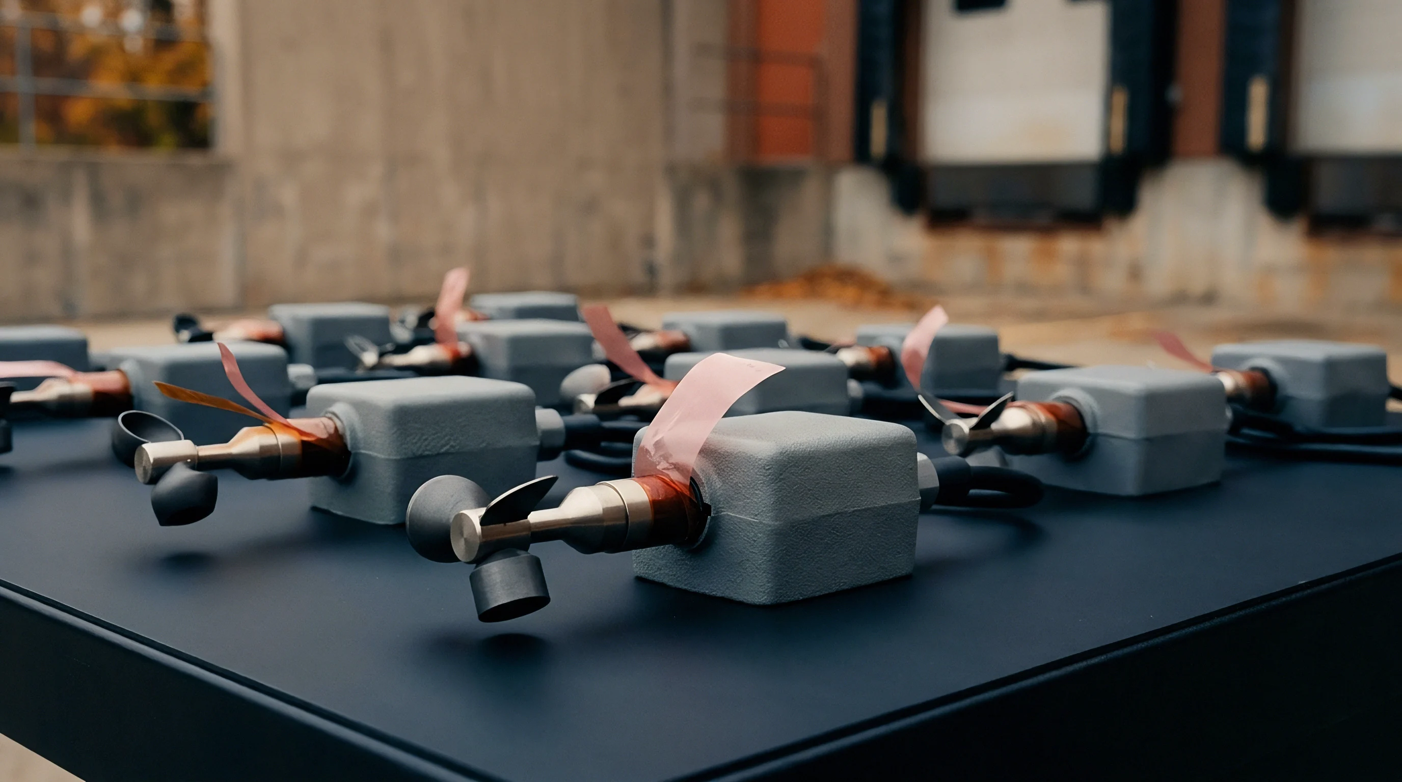
Digital Communications Protocols and Bus Integration
Digital interfaces replace analog voltage lines with serial communication networks embedded directly within the sensor package ASIC. Integrated I2C and SPI buses output fully compensated 14-bit to 24-bit pressure and temperature values. Digital communication eliminates host ADC error budgets, board-level voltage divider tolerances, and line-loss attenuation across cable runs.
Selecting between I2C and SPI interfaces alters pin counts, firmware overhead, and bus bandwidth limits.
| Parameter | I2C Standard Mode | I2C Fast Mode | SPI Mode 0 / Mode 3 | Analog Ratiometric |
|---|---|---|---|---|
| Bus Line Count | 2 (SDA, SCL) | 2 (SDA, SCL) | 4 (CS, SCLK, MISO, MOSI) | 1 (VOUT) |
| Maximum Clock Rate | 100 kHz | 400 kHz | 5.0 MHz to 10.0 MHz | N/A (Continuous) |
| Addressing Scheme | 7-bit Fixed / Config | 7-bit Fixed / Config | Hardware Chip Select | Point-to-Point |
| Maximum Cable Length | < 2 meters | < 0.5 meters | < 0.1 meters (On-board) | > 10 meters (Filtered) |
| Power Consumption | Low (< 1 mA active) | Low (< 1 mA active) | Moderate (< 3 mA active) | High (3 mA to 10 mA) |
I2C bus topologies reduce pin counts by sharing Serial Data (SDA) and Serial Clock (SCL) lines across multiple bus nodes. Open-drain output drivers require external pull-up resistors sized according to bus capacitance. Excessive bus capacitance slows signal rise times, causing communication timing faults.
Sizing pull-up resistor values balances signal edge speed against static power dissipation during low-bus logic states. Host controllers retrieve data from fixed or programmable 7-bit slave addresses stored in the ASIC EEPROM registers.
Firmware integration follows a sequential initialization protocol to clear host registers, configure measurement resolution, and trigger conversion cycles.
- Apply supply power within specified voltage rise limits and wait for the package ASIC internal power-on reset sequence to complete.
- Issue a start condition over the serial bus followed by the target sensor 7-bit device address and the write control bit.
- Write the measurement command byte to the sensor control register to initiate pressure and temperature sampling.
- Delay for the specified ASIC conversion duration based on chosen oversampling rates.
- Transmit the device address with the read control bit to request register contents.
- Clock out two to four bytes of pressure data followed by two bytes of integrated temperature sensor data.
- Validate the received checksum or cyclic redundancy check byte to verify packet data integrity before updating system control loops.
SPI buses provide faster throughput through dedicated full-duplex lines, reaching clock rates up to 10 megahertz. SPI configurations use an active-low Chip Select line to target specific sensors, avoiding address collision issues entirely. The four-wire footprint requires higher pin-count microcontrollers and increases PCB trace routing complexity compared to two-wire I2C implementations.
Properly sizing I2C bus pull-up resistors against trace capacitance maintains crisp rise times and prevents dropped packets across extended bus runs.


Drift

Mechanical Strain Transmission and Thermal Calibration
Silicon exhibits high piezoresistive coefficients, making it an exceptional sensing medium and a sensitive receiver of unwanted mechanical strain. Changes in ambient temperature generate mechanical forces within package materials that mimic applied fluid pressure. Piezoresistive coefficients themselves drop as temperature rises, reducing bridge sensitivity.
Uncompensated piezoresistive bridges experience full-scale output sensitivity shifts exceeding negative 0.2 percent per degree Celsius. Packages must combine mechanical strain relief with onboard electronic compensation to deliver stable outputs across temperature ranges.
Internal package stress pathways pass through the die-attach compound, substrate header, and encapsulation gel. Epoxy adhesives shrink during curing, creating localized compressive pre-loads on the silicon die. Over operational lifespans, the epoxy polymer matrix continues to relax, causing a slow continuous shift in the zero-pressure differential output.
Silicone die-attach materials offer lower elastic modulus values to absorb stress, but exhibit higher moisture absorption rates that introduce humidity-dependent zero offsets.
Integrated EEPROM calibration matrices inside the sensor package ASIC correct non-linear temperature errors using third-order polynomial math.
Factory calibration procedures map the mechanical and thermal responses of individual packaged dies before shipment. Sensors are cycled through multiple temperature and pressure states within automated thermal chambers. The package ASIC measures raw bridge output and internal diode temperature, storing unique correction coefficients into non-volatile EEPROM registers.
The host controller reads compensated digital values directly, eliminating manual circuit tuning and trimming operations during board production.

Long-Term Offset Stability and Error Budgets
Zero-point stability defines a sensor’s ability to retain its baseline output under zero applied gauge pressure over time. Soldering processes, thermal shock, and sustained pressure overloads push package materials past their elastic limits, producing permanent baseline offsets. Field failures often originate from gradual offset drift exceeding system tolerance thresholds rather than catastrophic silicon diaphragm fracture.
| Error Component | Uncompensated Die (%) | Standard Digital Package (%) | Precision Calibrated Package (%) |
|---|---|---|---|
| Non-Linearity (BSL) | ±0.25 FS | ±0.10 FS | ±0.05 FS |
| Thermal Hysteresis | ±0.50 FS | ±0.15 FS | ±0.05 FS |
| TC Offset (-20 to 85°C) | ±3.00 FS | ±0.50 FS | ±0.25 FS |
| TC Span (-20 to 85°C) | ±2.50 FS | ±0.50 FS | ±0.25 FS |
| Long-Term Drift (1 Year) | ±1.00 FS | ±0.25 FS | ±0.10 FS |
| Total Error Band (TEB) | ±7.25 FS | ±1.50 FS | ±0.70 FS |
Zero-point shifts exceeding 1.0 percent of full scale observed after board assembly often stem from improper reflow profiles and localized thermal gradients during soldering rather than package manufacturing defects.


Yield

Assembly Line Environment and Moisture Control
Surface-mount sensor packaging contains polymer materials, die-attach adhesives, and silicone gels that absorb moisture from surrounding ambient air. Exposing moisture-laden sensors to high temperatures during reflow soldering turns trapped water into high-pressure steam. Steam expansion creates internal delamination between the silicon die, substrate, and gel encapsulation.
This destructive mechanism, known as popcorning, destroys internal wire bonds and causes severe zero-point calibration shifts without visible cracking on the external package surface.
Moisture Sensitivity Level (MSL) ratings defined by JEDEC J-STD-020 govern component handling procedures on production lines. An MSL 1 rated package tolerates unlimited floor life at or below 30 degrees Celsius and 85 percent relative humidity. MSL 3 packages allow an exposed floor life of 168 hours after opening the sealed moisture barrier bag.
Production lines exceeding this time limit must bake packages in high-temperature ovens to remove trapped moisture before running surface-mount reflow operations.
Reflow soldering operations introduce aggressive chemical vapors from liquid flux formulations. No-clean flux residues containing organic acids migrate into unsealed top-port pressure cavities, depositing conductive films across wire bonds and open diaphragm surfaces. Ultrasonic cleaning baths break internal wire bonds and crack delicate silicon micromachined diaphragms through resonance fatigue.
Assembly procedures demand water-washable flux systems with restricted high-pressure spray orientations or force the use of protective wash covers during board washing cycles.
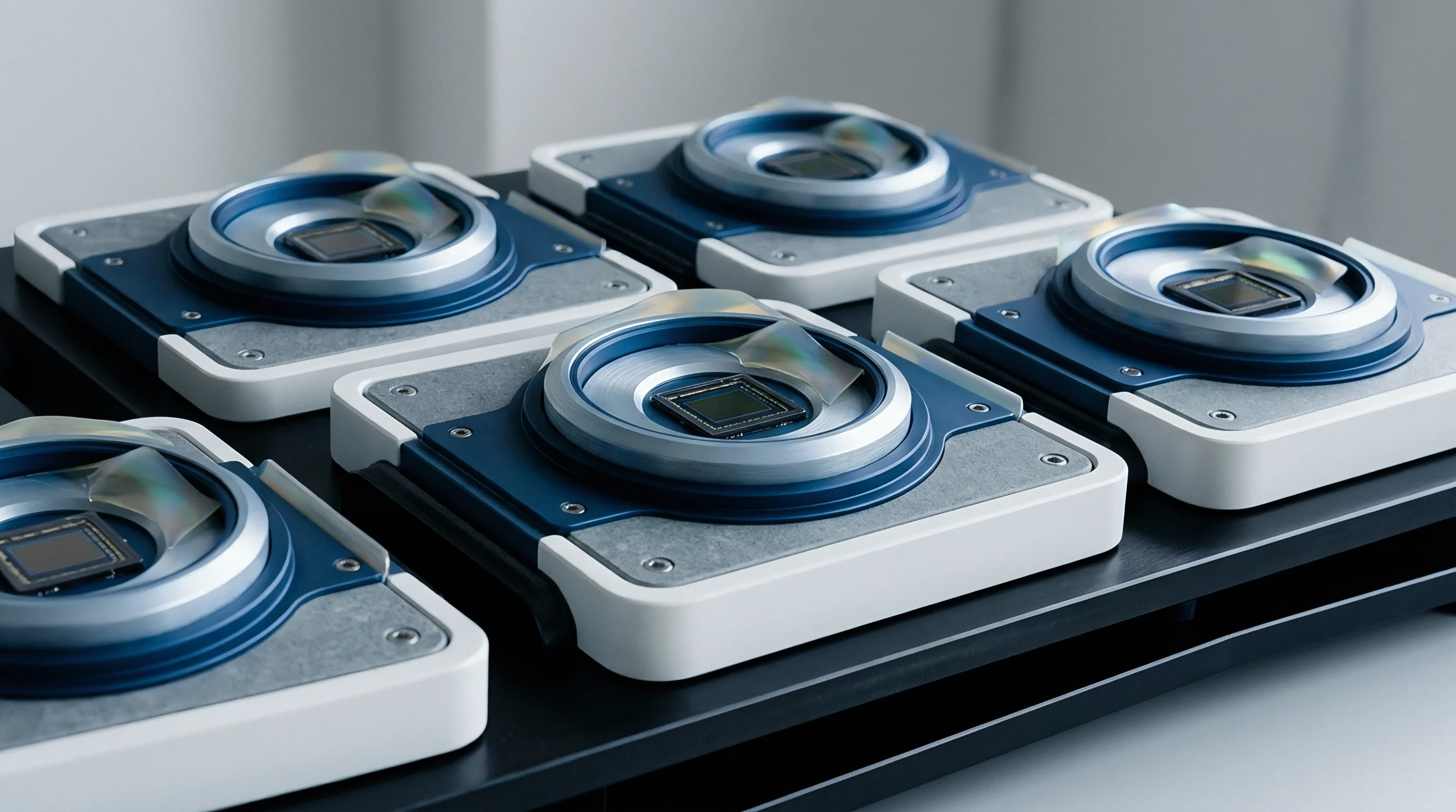
Incoming Inspection and Inline Verification Protocols
Receiving quality inspection protocols evaluate incoming component reels to identify material defects before surface-mount placement. Quality control teams verify tape-and-reel pocket tape dimensions, cover tape peel force, and humidity indicator card status inside sealed moisture barrier bags. Measuring baseline bridge resistance on sample parts from each lot confirms piezoresistive circuit continuity prior to line staging.
- Package Marking Verification ensures correct part numbers, pressure range designators, and lot traceability codes match incoming freight paperwork.
- Co-planarity Inspection measures bottom terminal alignment with optical vision systems to keep lead coplanarity within a strict 0.08-millimeter maximum tolerance band.
- Zero-Pressure Voltage Check samples un-soldered units inside a shielded chamber to confirm initial offset voltages sit within specified factory limits.
- Port Aperture Audit checks top and bottom pressure openings for physical debris, gel overflow, or plastic molding flash under stereo microscopes.
Section 4.2 of standard IPC-A-610 mandates that surface-mount component terminations show minimum 75 percent solder side-wall height and zero solder encroachment inside functional mechanical openings.

Tariff

Commercial Packaging Tiers and Unit Cost Mechanics
One bare silicon pressure sensor die reaches the commercial market inside multiple distinct package forms, spanning a twenty-to-one unit price spread. Raw piezoresistive die elements bought at wafer scale cost under fifty cents per unit in high volume. Packaging the bare die into an LGA surface-mount housing containing an ASIC adds leadframe costs, wire bonding time, and automated thermal calibration expense.
Casing the same silicon inside a stainless steel housing with an isolated oil-filled diaphragm elevates the assembly from a standard electronic component to a specialized industrial instrument.
Form factor selection dictates total landed bill-of-materials costs through both unit purchase price and required downstream board processing steps. Integrating a digital surface-mount sensor shifts signal conditioning, thermal testing, and calibration expense directly to the sensor manufacturer. Sourcing an uncompensated bare die drops initial component unit cost but transfers calibration testing, ASIC sourcing, and passive compensation network layout onto the board assembler.
| Package Variant | Unit Price 1k Vol ($) | Unit Price 100k Vol ($) | Minimum Order Qty | Engineering Bring-Up (Weeks) | Production Test Cost |
|---|---|---|---|---|---|
| Bare Uncompensated Die | 1.20 | 0.35 | 10,000 | 12 to 16 | High (Thermal Chamber) |
| LGA Digital SMT (Raw Gas) | 4.50 | 1.85 | 1,000 | 2 to 4 | Negligible (Pre-calibrated) |
| SOIC-8 Gel-Filled (Liquid) | 7.20 | 3.10 | 1,000 | 2 to 4 | Negligible (Pre-calibrated) |
| Integrated Cable Probe Module | 28.00 | 14.50 | 100 | 1 to 2 | Low (System Functional) |
| Stainless Isolated Transducer | 85.00 | 42.00 | 25 | 1 | Zero (Direct Plug-in) |

Make-or-Buy Decision Boundaries and Sourcing Strategy
Volume thresholds determine whether designing a custom module-on-board architecture beats buying off-the-shelf pre-calibrated digital packages. Developing a custom sensor module around a bare piezoresistive die demands significant upfront capital expenditure. Non-recurring engineering (NRE) costs for custom substrate tooling, gel dispense equipment, and automated pressure-temperature test chambers typically exceed 150,000 US dollars.
Software development for host-side thermal compensation routines adds firmware engineering weeks to project schedules.
Annual production volumes below 50,000 units favor fully integrated, pre-calibrated digital surface-mount packages. Higher component unit costs are offset by eliminating factory calibration equipment, reducing board test times to simple digital query commands, and avoiding specialized gel encapsulation machinery. Higher volume runs above 250,000 units justify amortizing NRE and calibration capital investments across large production volumes, allowing bare die architectures to unlock substantial unit cost reductions.
Sourcing strategies must account for package lifecycle notices and distributor stocking trends. Standard SOIC-8 and QFN packaging variants enjoy multi-source availability and long production lifespans across multiple semiconductor foundries. Proprietary custom molded module housings risk single-source supply chain lock-in.
When a niche sensor packaging line reaches end-of-life status, re-engineering a custom land pattern and updating host firmware forces expensive product re-certification cycles across end-market industrial and medical installations.