Transducer Signal Degradation in Industrial Packaging under Thermal Cycling
Thermal expansion mismatches in transducer packaging transfer mechanical stress to silicon dies, driving zero offset drift and signal hysteresis under thermal cycling.


Die
Silicon MEMS elements convert mechanical strain into electrical impedance shifts through piezoresistive bridges. Packaging materials surround these sensing structures, introducing mechanical coupling that alters signal output over operational lifetimes. Temperature swings force structural materials to expand and contract at differing rates.
Die stresses multiply. This mismatch induces parasitic strain across the active sensing surface, causing zero-point offset shifts and span calibration drift.

Mechanical Stress Transfer Mechanics
Transfer molding materials encapsulate delicate pressure-sensing structures to protect against ambient contamination. Mold compounds exhibit high elastic modulus values alongside volumetric thermal contraction during cure phases. Solder joints flex.
Residual mechanical stress acts directly upon the embedded silicon micro-machined diaphragm, biasing the internal Wheatstone bridge. Differential expansion rates between the organic substrate and the silicon die create a triaxial stress field across the package footprint.
When an industrial sensor experiences thermal cycling between minus 40 degrees Celsius and 125 degrees Celsius, package component dimensions change continuously. The die-attach epoxy layer absorbs a fraction of this strain, yet stiff adhesives transmit compressive shear directly to the silicon perimeter. The internal strain profile alters the piezoresistive coefficients of the doped silicon traces.
The piezoresistive response drifts, appearing at host electronics as a false change in measured pressure or acceleration.
- Die-attach epoxy compliance modulates stress transmission from the substrate to the silicon substrate, where low-modulus silicone formulations reduce shear transfer at the cost of higher moisture permeability.
- Mold compound thermal expansion matches copper leadframe material behavior closely, reducing lead frame bending while generating elevated compressive force on internal die surfaces.
- Silicon diaphragm geometry concentrates thermomechanical stress at thin edge boundaries, accelerating offset drift in low-pressure piezoresistive sensing structures.
- Substrate glass transition temperature governs material stiffness changes, causing sharp shifts in drift rates once ambient exposure exceeds polymer transition limits.

Coefficient Mismatch at Mold Interfaces
Substrate differential expansion generates planar shear across organic die-attach adhesives. Silicon possesses a thermal coefficient of expansion near 2.6 ppm per Kelvin, whereas standard FR4 circuit boards expand at roughly 14 to 17 ppm per Kelvin. High-density transfer molding compounds typically fall between 8 and 12 ppm per Kelvin below their glass transition temperature.
Operating environments with wide temperature bands force these bonded layers to shear against each other at every interface.
Over hundreds of thermal cycles, interfacial stresses exceed the shear strength of organic adhesives. Micro-cracks initiate within the die-attach matrix, reducing mechanical support uniformity across the silicon base. As localized shear stress relaxes unevenly, the sensor zero-offset point drifts irreversibly.
Sensor packaging that lacks balanced mechanical buffering exhibits continuous calibration loss throughout its deployment life.


Hysteresis
Non-reversible signal shifts manifest when thermal excursions push packaging polymers past their elastic yield limits. Plastic deformation inside internal adhesives prevents the sensing element from returning to its original physical state upon returning to baseline temperatures. Thermal hysteresis remains.
The output signal displays a memory effect, where measured values depend upon whether the current temperature was reached from a cold state or a hot state.
A piezoresistive silicon die packaged in standard transfer-molded epoxy exhibits an uncompensated zero-point offset shift up to 1.8 percent full scale span following 500 thermal cycles between minus 40 degrees Celsius and 125 degrees Celsius.

Zero-Point Offset and Span Deviation
Continuous temperature excursions disturb the balanced Wheatstone bridge resistors printed on silicon. Offset drift alters zero-pressure baseline readings, while span deviation changes the full-scale output gain factor. Offset error accumulates.
Polymer viscoelastic relaxation occurs over prolonged dwell times at high temperatures, causing time-dependent baseline drift that evades standard two-point calibration routines implemented at assembly.
Span degradation develops when packaging mechanical stress changes the piezoresistive sensitivity factors of silicon traces. When ambient temperatures drop, the mold compound contracts faster than silicon, applying isotropic compression that alters baseline electrical resistance. Upon re-heating, incomplete viscoelastic recovery leaves residual stress trapped within the package body, permanently biasing output voltages.
- Mount the packaged sensor inside an environmental test chamber on a rigid test fixture to minimize external PCB flexure during temperature swings.
- Connect a regulated, low-noise DC power supply and attach precision digital voltmeters directly across signal output pins using shielded copper leads.
- Ramp chamber ambient temperature from 25 degrees Celsius down to minus 40 degrees Celsius at a controlled rate of 2 degrees Celsius per minute.
- Dwell at minus 40 degrees Celsius for 60 minutes while logging zero-input baseline output voltage at 10-second sampling intervals.
- Ramp chamber temperature to 125 degrees Celsius at 2 degrees Celsius per minute, holding for 60 minutes to capture high-temperature span values.
- Return ambient temperature to 25 degrees Celsius and record the final uncompensated zero-point voltage to quantify thermal hysteresis offset.

Measurement and Test Regimes
Environmental chambers cycle assemblies between defined thermal limits while logging bus outputs. Quantifying package degradation requires isolation of mechanical strain effects from intrinsic silicon semiconductor drift. Accelerated stress testing subjects parts to extreme temperature change rates up to 10 degrees Celsius per minute, forcing rapid stress buildup across material boundaries.
| Material Layer | CTE Below Tg (ppm/K) | Young Modulus (GPa) | Mechanical Stress Contribution |
|---|---|---|---|
| Silicon Monocrystalline Die | 2.6 | 130 to 180 | Primary transducer element baseline |
| Die-Attach Silicone Adhesive | 150 to 300 | 0.001 to 0.010 | Low shear strain transfer buffer |
| Die-Attach Epoxy Adhesive | 40 to 65 | 3.0 to 8.0 | High mechanical coupling and stress transfer |
| Epoxy Mold Compound (EMC) | 8 to 12 | 15 to 25 | Compressive package body encapsulation |
| FR4 Substrate Circuit Board | 14 to 17 | 18 to 22 | External printed circuit interface board |
Quantification of degradation parameters relies on continuous monitoring during thermal transitions. Static pre-test and post-test measurements fail to capture transient peak stresses that occur mid-ramp. Thermal stress cycles destabilize Wheatstone bridge geometry, degrading signal-to-noise ratios across industrial control loops.
Ignoring thermomechanical package mechanics during sensor sourcing leads to unexpected field failures and costly recalibration cycles.


Gel
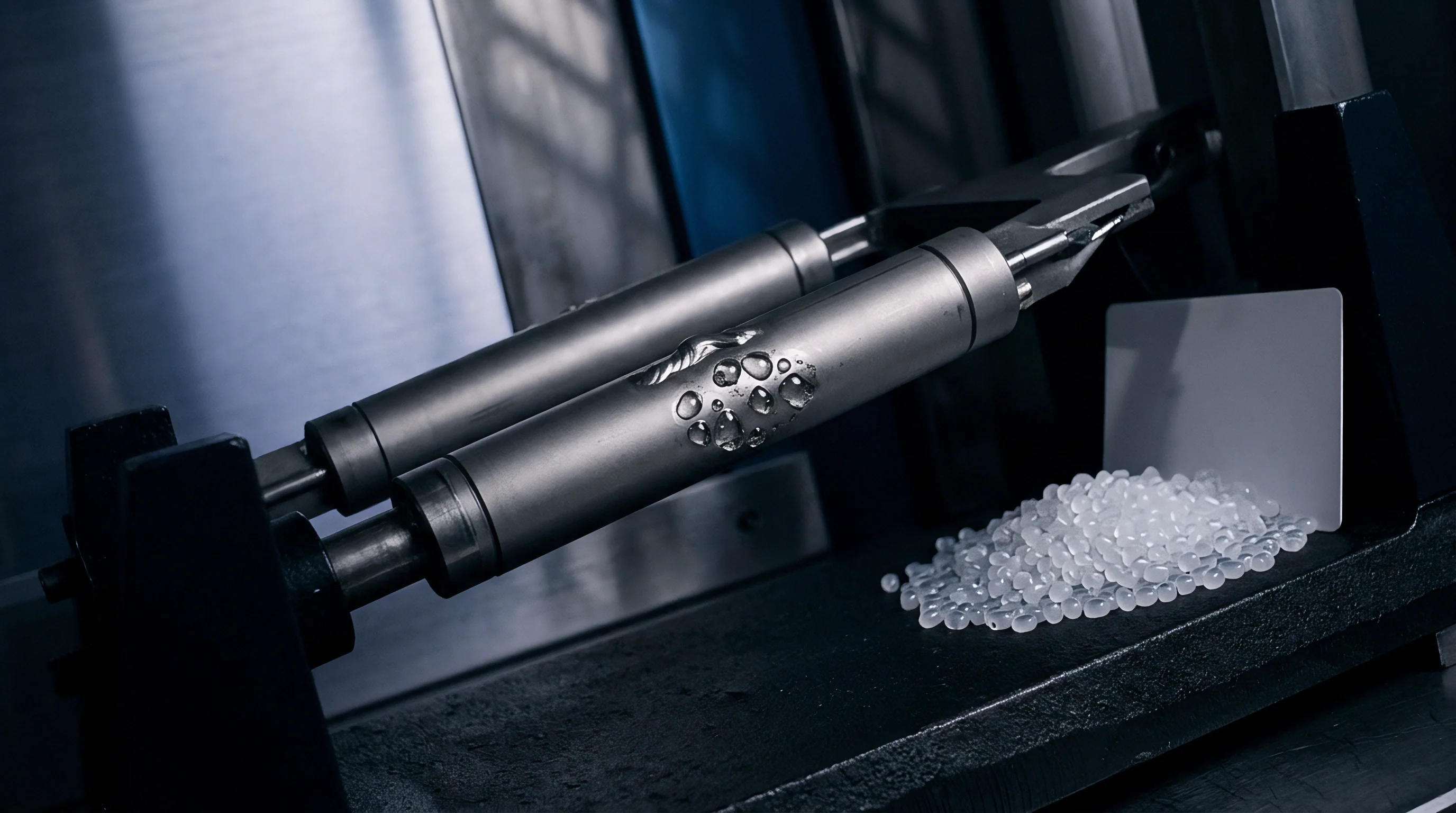
Fluorosilicone potting compounds protect sensor diaphragms from aggressive chemical vapors. Media-isolated pressure transducers rely on soft gel fill to transmit fluid pressure directly to the delicate silicon diaphragm while barring corrosive liquids. Silicone gel migrates.
Under repeated thermal cycling, cross-linked polymer networks inside gels break down, altering mechanical compliance and signal transmission fidelity.
Protective Media Characteristics
Encapsulation polymers maintain elastomeric softness down to sub-zero industrial operating temperatures. The glass transition point of standard silicone gel sits near minus 120 degrees Celsius, allowing flexible pressure transfer across broad operating windows. Fluorosilicone variants offer superior resistance to solvent swelling, though their higher density increases mechanical damping at high frequency signal inputs.
Fluorosilicone gel fills insulate sensing diaphragms from chemical attack while transferring mechanical shear stress to die edges during extreme cold dwell periods.
Temperature swings induce significant volume expansion and contraction within gel-filled cavities. Stainless steel housings exhibit a thermal expansion coefficient around 16 ppm per Kelvin, whereas silicone gels expand at rates exceeding 300 ppm per Kelvin. This massive expansion differential forces gel media against internal cavity walls during thermal ramps, exerting hydrostatic pressure on active sensing surfaces independent of actual process media pressure.

Delamination Risks at Cavity Walls
Repeated expansion cycles weaken the adhesive interface between housing sidewalls and soft potting compounds. Interfacial void formation allows gel material to shift inside the cavity, altering the effective oil volume pressing against the sensor diaphragm. Cavity pressure shifts.
Internal bubble formation occurs when dissolved gases exsolve from gel matrices during high-temperature exposure under partial vacuum conditions.
Suppliers often defend zero-point drift by claiming that gel-filled sensor cavities self-heal after thermal stabilization. Field experience proves that soft gel formulations develop localized stress pathways after repeated freezing cycles, generating permanent offset shifts that bypass internal thermal compensation algorithms.


Fatigue
Surface-mount solder joints experience cyclic plastic deformation during environmental temperature ramps. Package CTE differences relative to the main motherboard generate high mechanical shear strain across solder fillets. Solder joints flex.
Leadless package architectures such as QFN and LGA concentrate strain directly beneath corner interconnect terminations, accelerating metallurgical fatigue cracks.
Compliance with AEC-Q100 Grade 1 thermal cycling standard JESD22-A104 dictates less than 0.25 percent span shift across 1000 temperature cycles to prevent sensor re-qualification penalties.

What Drives Long-Term Zero-Point Offset Drift?
Structural relaxation inside metal interconnects causes irreversible baseline shifts across sensor operation. Lead-free SAC305 solder undergoes creep deformation at room temperature due to its high homologous operating temperature. Microstructural coarsening transforms fine grain boundaries into large grain structures, reducing fatigue resistance over successive thermal cycles.
Solder fatigue develops.
As micro-cracks propagate through solder joints, ground loop impedance and contact resistance increase unpredictably. Analog signal paths suffer voltage drops that corrupt low-level sensor outputs prior to amplification. Ground offset changes appear directly as measurement error in single-ended analog sensor architectures.
- Intermetallic compound growth at solder-copper pad interfaces forms brittle Cu6Sn5 and Cu3Sn layers that fracture under mechanical thermal stress.
- Corner joint strain concentration accelerates crack initiation on leadless packages lacking compliant outer metal leads.
- PCB board flexure deformation couples external mechanical bending directly into the sensor packaging substrate.
- Thermal ramp speed acceleration increases plastic strain energy density per thermal cycle, shortening overall interconnect cycle life.

Packaging Structural Comparisons
Quad Flat No-lead packages exhibit higher stress concentration than leads-bearing Small Outline packages. Compliant gull-wing leads absorb substrate movement through structural flexure, reducing stress transferred to internal die bonds. Package selection balances compact board area requirements against long-term signal stability under harsh thermal environments.
| Package Type | Zero Offset Drift (% FSS) | Span Shift (% FSS) | Primary Degradation Mode | Unit Sourcing Price Premium |
|---|---|---|---|---|
| SOIC-16 (Gull-Wing Leads) | 0.08 to 0.15 | 0.05 to 0.12 | Lead frame flex relaxation | Baseline 1.0x |
| QFN-24 (Leadless Surface Mount) | 0.35 to 0.85 | 0.25 to 0.50 | Solder joint fatigue and planar die tilt | 1.15x |
| LGA-12 (Bottom Land Array) | 0.45 to 1.10 | 0.30 to 0.65 | Solder pad cracking and corner stress | 1.25x |
| TO-39 (Hermetic Metal Can) | 0.02 to 0.05 | 0.01 to 0.04 | Glass-to-metal seal creep strain | 3.80x |
| Cabled Probe Module (Housed) | 0.05 to 0.10 | 0.03 to 0.08 | Cable potting stress relaxation | 8.50x |
| Data synthesized across accelerated thermal cycling per JEDEC JESD22-A104 conditions; values reflect uncompensated analog die outputs. | ||||
How much signal degradation stems from internal die bond degradation versus external board-level solder cracking in leadless surface-mount sensor modules?


Trim
Embedded digital signal processors adjust internal amplifier gain to offset raw sensor drift. Modern smart transducers carry integrated digital trim registers, reading internal temperature sensors to apply polynomial correction formulas in real time. Interface speed drops.
Digital interfaces mask minor mechanical stress effects, but severe packaging strain causes non-linear output errors that exceed mathematical correction capacity.
Digital interface compensation registers lose residual calibration accuracy when thermomechanical package stress exceeds the linear range of internal strain-gauge arrays.

Digital Compensation and Bus Limits
System firmware reads multi-point calibration tables to calculate corrected output pressure values. Internal factory calibration coefficients locked into EEPROM during manufacturing assume stable mechanical coupling between package and die. Wire bonds lift.
When thermal cycling alters package mechanical stress state, factory correction coefficients fail to match the shifted stress profile, causing residual calibration errors.
Digital buses like I2C and SPI transmit compensated sensor data directly to host controllers without analog signal line loss. High bus capacitance and thermal drift on pull-up resistors degrade digital edge transition times. Signal corruption occurs when long bus wiring operates in high-temperature environments, causing dropped communications or frame checksum errors.
- Polynomial order depth limits firmware compensation capability when packaging thermal hysteresis introduces higher-order non-linearities.
- On-chip temperature sensor placement introduces measurement phase lag if the thermal sensor sits away from active piezoresistive bridges.
- EEPROM memory retention faces degradation under continuous high-temperature exposure, threatening stored calibration matrix integrity.
- Bus line pull-up sizing requires adjustment to handle temperature-dependent pin capacitance changes across long sensor wiring runs.

Interface Protocol Vulnerabilities
Serial communication links transmit corrected 16-bit readings to host controllers under harsh noise conditions. Digital protocols eliminate line attenuation risks inherent to 0-10V or 4-20mA analog output loops. Firmware week allocations grow rapidly when custom driver stacks must process error detection flags and dynamic recalibration loops forced by thermomechanical sensor drift.
| Interface Specification | Data Resolution | Firmware Bring-Up (Weeks) | Temperature Drift Susceptibility | Sourcing Impact |
|---|---|---|---|---|
| Unamplified Ratiometric Analog | Continuous | 0.5 to 1.0 | High (Direct stress and drift transmission) | Lowest unit cost, high host burden |
| Amplified 0.5V to 4.5V Analog | Continuous | 0.5 to 1.0 | Moderate (Internal amp drift added) | Low unit cost, simple interface |
| I2C Digital Bus (400 kHz) | 12 to 16 Bits | 2.0 to 4.0 | Low (Digitized at sensor die) | Moderate cost, short wire limit |
| SPI Digital Bus (10 MHz) | 14 to 24 Bits | 3.0 to 5.0 | Low (Digitized at sensor die) | Moderate cost, extra line pins |
| SENT Protocol (SAE J2716) | 12 to 16 Bits | 4.0 to 6.0 | Very Low (Robust point-to-point digital) | Higher cost, automotive grade |
High-resolution digital conversion done directly inside the transducer package isolates analog signal degradation to the silicon surface, leaving bus stability and calibration matrix freshness as the governing operational factors.


Warranty
Sourcing agreements specify acceptable signal drift parameters over specified temperature profiles. Sourcing practices protect production programs by embedding maximum zero-offset drift caps directly into component purchase contracts. Span error doubles.
Supplier guarantees based solely on static room-temperature testing leave buyers exposed to assembly yield losses when thermal cycling occurs in field deployments.

Procurement Risk Mitigation
Sourcing contracts enforce rigorous lot acceptance thresholds before releasing production shipments. Procurement specifications require certified batch data demonstrating thermal cycle testing per JEDEC standards. Unqualified packaging changes made by component foundries alter mechanical strain performance without altering electrical pinouts, making incoming component screening mandatory.
Audit procedures verify that transducer manufacturers maintain process control over die-attach epoxy viscosity, mold compound cure schedules, and gel fill dispensing volumes. Variability in internal assembly processes creates severe lot-to-lot thermal drift discrepancies. Clear contract language provides recourse when field component failure rates exceed qualification projections.

Cost Analysis across Package Form Factors
Packaging selections alter both raw sensor unit price and downstream manufacturing yield metrics. Bare silicon sensing dies carry minimal upfront cost but shift encapsulation, gel fill, and thermal calibration burdens entirely onto the buyer board assembly line. Pre-calibrated, housed transducer modules command significant price premiums while shifting thermomechanical reliability risk directly back to the vendor.
The purchase agreement stipulates that thermal drift exceeding 0.20 percent full scale span across 500 qualification cycles triggers automatic lot rejection and supplier-funded root-cause failure analysis.