Interface Mechanism
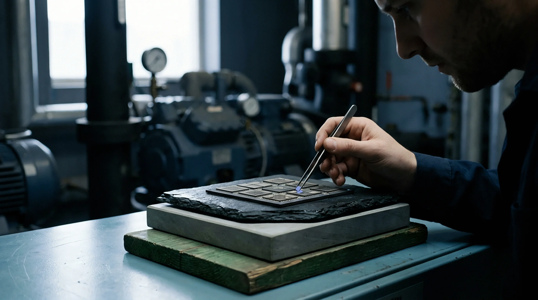
Field assisted thermal sealing creates a permanent connection between a silicon wafer and a glass substrate. In the cleanroom environment, anodic bonding applies high voltage across the assembly while the parts are held at an elevated temperature. This potential difference drives mobile sodium ions within the glass away from the interface.
The resulting negative charge density at the junction creates a strong electrostatic force that brings the surfaces into intimate contact. Oxygen ions then migrate to form a thin silicon dioxide layer between the two members. This hermetic seal remains stable under high pressure and variable atmospheric conditions.
The limit of this method occurs when the surface roughness of the material prevents the initial contact sequence required for the formation of atomic bonds.
Thermal Calibration
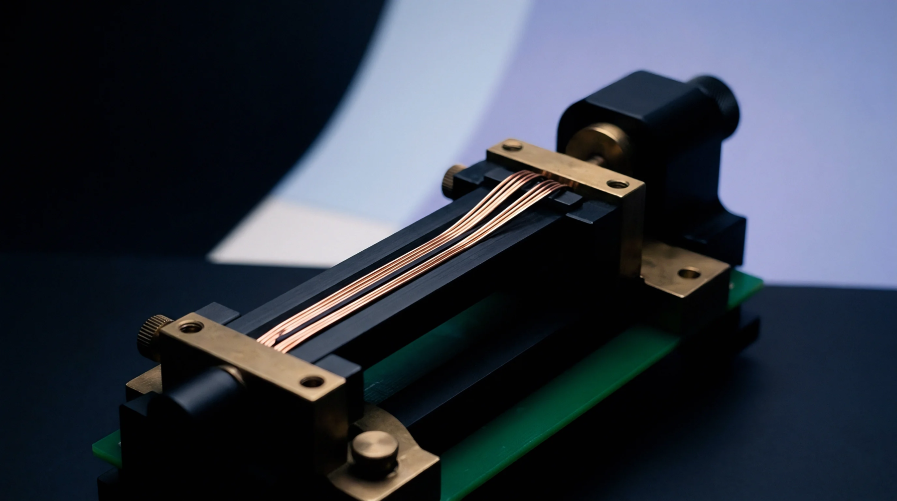
Heat management determines the residual stress remaining in the package after it cools to room temperature. During the cycle, anodic bonding requires precise synchronization between the heater plates and the high voltage source. Even a small difference in the expansion rates of the silicon and glass leads to warping or cracking.
Selection of the glass type is restricted to materials like borosilicate that match the thermal properties of the semiconductor. Sourcing these wafers involves verifying the flatness through interferometry before they enter the bonding chamber. If the glass contains too few alkali ions, the bonding current never reaches the magnitude needed for a solid joint.
Conversely, an excess of mobile ions can lead to electrical leakage that damages sensitive integrated circuits nearby.
Process Stability
Voltage levels must be adjusted to account for the thickness of the glass and the desired strength of the connection. For standard MEMS production, anodic bonding typically proceeds at levels between four hundred and one thousand volts. Measuring the cumulative charge transfer during the process indicates whether the contact has covered the entire surface area.
If the current drops faster than expected, it suggests that air pockets remain trapped in the interface. These voids act as weak points that might fail during centrifugal testing or thermal cycling. Manufacturers often qualify the bond through a pull test or by inspecting the fringe patterns with optical microscopy.
Stable bonding processes show a characteristic downward curve in the current monitor over time. This trend confirms the depletion of ions at the bonding front.
Assembly Verification
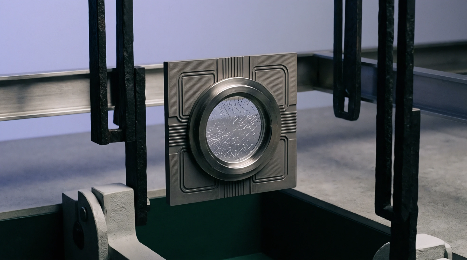
Visual inspection through the transparent glass provides immediate confirmation of the seal consistency. If the process is successful, anodic bonding produces a characteristic grey or clear interface without visible gas bubbles. Any interference from dust particles appears as dark Newton rings surrounding a central defect.
These gaps break the hermetic seal and allow moisture to penetrate the device cavity over time. Testing for the hermeticity often involves a fine leak test with helium or a gross leak test using fluorocarbon immersion. Calibration of the bonding equipment includes checking the pressure of the contact pins to ensure even distribution across the entire wafer surface.
High precision in these parameters prevents local hotspots that could melt the glass or damage the circuit patterns. The technique is essential for the protection of internal sensor components from external contaminants.