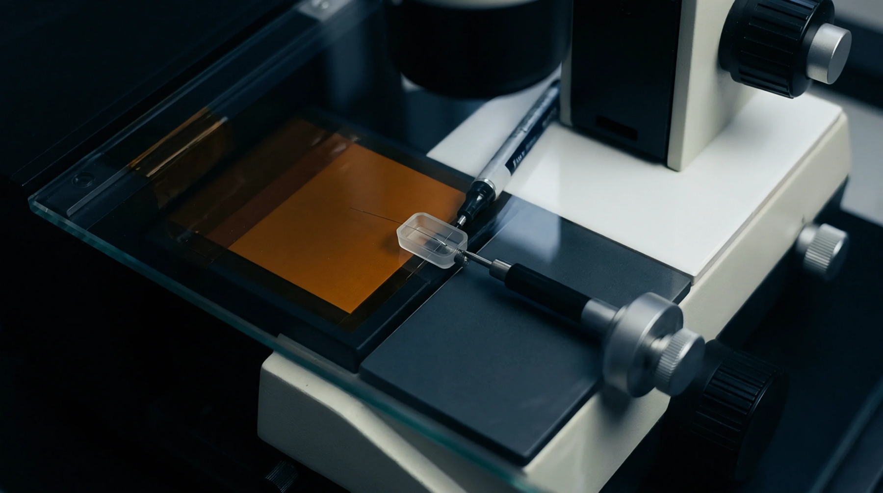
Mechanical Substrate
Micromachined support structures in semiconductor sensors are designed to isolate the active sensing element from external mounting stresses. This structural feature, known as a silicon pedestal, provides a rigid and chemically compatible base for pressure or temperature chips. It is fabricated using silicon etching techniques.
Thermal Isolation
Heat transfer between the packaging housing and the active sensor die is minimized by reducing the contact area. The silicon pedestal acts as a thermal bottleneck, which reduces the response time and prevents temperature gradients from affecting the measurements. This isolation ensures that the die remains closer to the temperature of the fluid being measured.
Stress Isolation
Mechanical strains originating from the mismatch in thermal expansion between the sensor housing and the silicon die are absorbed by the support structure. By mounting the sensing element on a silicon pedestal, the die is lifted away from the solder joint or adhesive layer that connects the assembly to the metal housing. This elevation prevents package-induced stress from bending the die, which would otherwise cause piezoresistive offsets in the output signal.
Such configuration is essential for maintaining sub-millibar stability in precision pressure transmitters.
Mounting Limit
Physical dimensions of the support structure must be optimized to prevent resonant vibrations in high-frequency environments. If the pedestal is made too tall or too narrow, it may fracture under high acceleration or shock. This structural constraint forces a compromise between mechanical strength and stress isolation.