Interfacial Shear Stress Transfer Mechanics in Silicon Piezoresistive Transducers
Interfacial shear stress transfers package thermal mismatch into piezoresistor bridges, requiring glass pedestals to prevent unrecoverable zero-point drift.


Anchor
A silicon die bonded to an alumina header with a thirty-micrometer layer of unfilled epoxy undergoes an uncalibrated zero-point shift when thermal cycles drive shear across the joint. The piezoresistive sensing bridge responds directly to mechanical strain, recording any force transmitted through the sub-die boundary alongside fluid pressure. A transducer vendor quotes a static error band of 0.10 percent full-scale output across twenty-five degrees Celsius.
The same transducer routinely displays an offset wandering across 0.75 percent full-scale output when cycled between minus forty and eighty-five degrees Celsius. Factory calibration at room temperature records an intact mechanical equilibrium that alters as the packaging materials relax under temperature gradients. The bridge cannot separate pressure-induced membrane deflection from packaging-induced shear loading.
Piezoresistors implanted along the (110) crystallographic directions of a (100) silicon diaphragm experience resistance changes proportional to longitudinal and transverse stresses. The piezoresistive coefficients relate fractional resistance variation directly to in-plane normal stresses. Non-uniform interfacial shear stresses along the die-attach plane induce bending moments and parasitic in-plane normal stresses across the diaphragm edges.
When shear stress transfers from the package through the die thickness, the piezoresistive elements register an artificial differential signal. Transducer packaging isolates the die from external housing deformations while providing an absolute anchor against media pressure. This dual requirement creates a mechanical compromise.
Die-attach shear stress transfers into diaphragm edge bending moments that directly alter piezoresistor zero-offset balances across thermal cycles.
The mechanical stack consists of the silicon sensing die, an intermediate joining material, and a structural header or port. Common header materials include covar, stainless steel alloys, and alumina ceramic. The thermal expansion coefficient of monocrystalline silicon sits near 2.6 parts per million per Kelvin.
Alumina ceramic exhibits approximately 7.0 parts per million per Kelvin. Martensitic or austenitic stainless steels range from 10.5 to 16.0 parts per million per Kelvin. A temperature shift generates differential expansion between the die and header, forcing the intermediate adhesive or solder layer to sustain high shear strains.
The magnitude of shear stress transferred into the die depends on the adhesive layer thickness, its effective shear modulus, and the distance from the die center.
Procurement teams often treat zero-temperature drift as an electronics problem solved by digital signal processors or lookup tables in application-specific integrated circuits. The error originates as an interfacial stress distribution displaying spatial asymmetry and viscoelastic time-dependence. When the adhesive creeps, the offset changes at constant temperature, rendering static lookup matrices invalid over extended deployment intervals.
Purchasing piezoresistive dies with tighter intrinsic bridge balancing does not resolve drift caused by packaging shear mechanics. An engineering buyer must inspect the joint stack parameters, interface compliance, and assembly metallurgy to verify sensor stability.


Joint
Stress transfer across an adhesive bond obeys lap-joint shear lag mechanics governed by differential thermal contraction. Volkersen formulations adapted to micro-electro-mechanical assemblies quantify the shear stress distribution along the die-substrate boundary. Shear stress reaches zero at the die neutral center and climbs to its maximum at the perimeter corners.
A silicon die measuring three millimeters on a side concentrates shear at its edges, transmitting parasitic bending moments inward toward the thin micromachined diaphragm. The mechanical load transfer parameter depends upon the ratio of adhesive shear modulus to adhesive bondline thickness.

Shear Lag Governing Formulations
Mathematical representation of the interfacial shear stress distribution follows shear lag differential equations balancing axial forces in the die and substrate against shear deformation in the adhesive. Considering a die of length 2L, thickness t_s, and Young’s modulus E_s, bonded via an adhesive of thickness t_a and shear modulus G_a to a substrate of thickness t_sub and modulus E_sub, the interfacial shear stress tau(x) at distance x from the die center satisfies:
tau(x) = (Delta_alpha Delta_T G_a / (beta t_a)) (sinh(beta x) / cosh(beta L))
The characteristic shear lag parameter beta is defined by the mechanical stiffness values of the bonded assembly components:
beta = sqrt((G_a / t_a) (1 / (E_s t_s) + 1 / (E_sub t_sub)))
Delta_alpha represents the thermal expansion coefficient mismatch between substrate and silicon, while Delta_T denotes the temperature excursion from the zero-stress curing state. Peak interfacial shear stress occurs at the extreme boundary where x equals L. The ratio of sinh(beta L) to cosh(beta L) approaches unity for large values of beta L, making peak shear stress scale directly with the thermal expansion gap and the square root of the adhesive shear modulus. Thick bondlines reduce beta, lowering the peak edge shear and spreading the load across a wider zone.
The physical displacement of the die surface causes normal stress variations along the active sensor plane. Integrating interfacial shear stresses over the distance from the edge to the diaphragm perimeter yields the net transmitted parasitic in-plane load. When die mounting exhibits voiding or bondline tilt, beta varies across the die footprint, breaking structural symmetry.
Asymmetric stress distributions convert pure in-plane forces into out-of-plane warpage. Diaphragm warpage shifts the piezoresistor positions relative to the neutral bending axis, producing offset errors that mimic real applied media pressure.
| Bonding Material Class | Young’s Modulus (GPa) | Shear Modulus (GPa) | Thermal Expansion (ppm/K) | Characteristic Shear Lag Beta (mm^-1) | Zero-Point Stability Metric |
|---|---|---|---|---|---|
| Unfilled Die-Attach Epoxy | 2.8 | 1.0 | 55.0 | 2.15 | Unstable across thermal cycling |
| Silver-Filled Conductive Epoxy | 6.5 | 2.4 | 35.0 | 3.32 | Moderate viscoelastic drift |
| Soft Silicone Elastomer | 0.005 | 0.0017 | 300.0 | 0.09 | High mechanical isolation |
| Gold-Tin Eutectic Solder (80Au/20Sn) | 68.0 | 25.5 | 16.0 | 10.85 | High zero-point stability |
| Anodic Bonded Borosilicate Glass | 64.0 | 26.7 | 3.25 | 0.31 | Hermetic metrological reference |
Soft silicone elastomers decouple the silicon die from housing expansion by reducing the shear modulus to fractional megapascal ranges. The characteristic parameter beta drops below 0.1 inverse millimeters, eliminating edge stress concentration. Elastomeric adhesives introduce gross compliance that allows the die to tilt under high acceleration or dynamic pressure pulsations.
Gold-tin eutectic solders offer zero viscoelastic relaxation, locking the assembly into an elastic state where thermal expansion mismatches generate high interfacial shear stresses exceeding eighty megapascals. Borosilicate glass constraint pedestals match the silicon expansion coefficient closely, minimizing Delta_alpha to hold edge shear stresses below five megapascals without elastomeric creep.
Die-attach adhesives alter their properties across normal transducer operating temperatures. An epoxy with a glass transition temperature of 120 degrees Celsius maintains a glassy modulus of several gigapascals throughout room temperature evaluation. Deploying that transducer into an automotive coolant or industrial steam monitoring line past 130 degrees Celsius drops the adhesive modulus by two orders of magnitude into its rubbery regime.
This glass transition shifts beta abruptly, shifting the mechanical boundary conditions of the diaphragm and altering the sensor span calibration. Downward thermal excursions into minus forty degrees Celsius increase epoxy brittleness, amplifying peak shear stresses and elevating bond cracking risks.
Adhesive curing cycles establish the baseline zero-stress temperature. If a silver-filled epoxy crosslinks at 150 degrees Celsius, the assembly enters room temperature service under steady compressive stress driven by substrate contraction. Room temperature storage maintains high shear stress along the joint interface for the lifetime of the component.
Room temperature vulcanizing adhesives reduce this built-in thermal stress but exhibit moisture absorption that plasticizes the polymer chain network. Transducer manufacturers selecting bonding agents balance elastic mismatch against time-dependent material relaxation.
A supplier will state that modern automated dispensing maintains absolute bondline uniformity across production volumes.

Creep
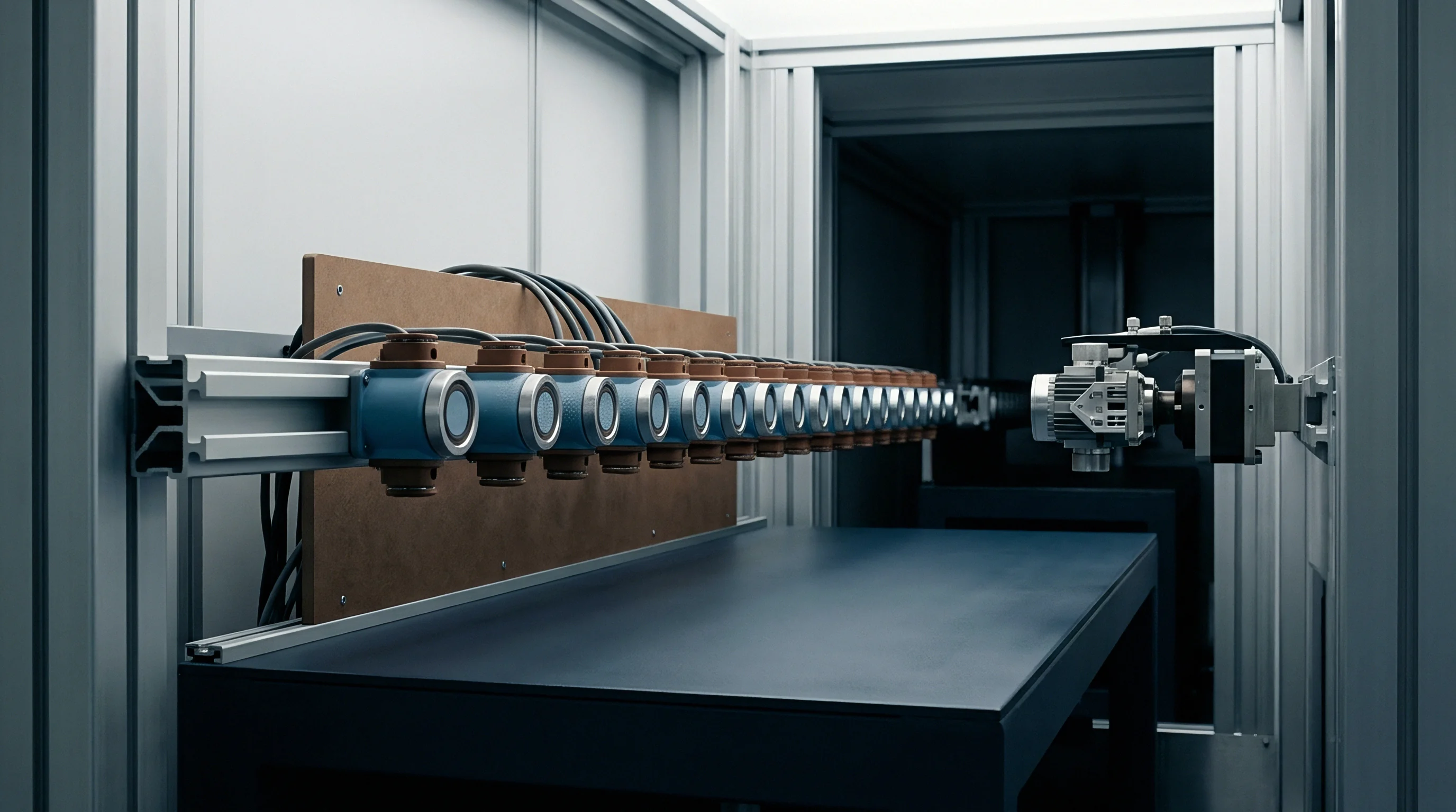
Polymer die-attach layers undergo continuous molecular chain rearrangement under sustained interfacial shear stress. This time-dependent relaxation converts elastic mechanical strain into unrecoverable plastic strain, changing the stress field transferred to the piezoresistive bridge. When an industrial transmitter remains at eighty degrees Celsius under steady atmospheric pressure, the recorded digital output slowly drifts over weeks of continuous operation.
The instrument housing expands, creating sustained shear stress in the adhesive that dissipates via primary and secondary creep mechanisms. Metrology laboratories recalibrating pressure transmitters after eighteen months routinely observe that zero-point errors exceed the original factory accuracy rating even when the sensor experienced no overload events.

Viscoelastic Shear Relaxation Models
Viscoelastic shear stress dissipation within polymer joints follows Kohlrausch-Williams-Watts stretched exponential kinetics or generalized Maxwell configurations. The relaxation modulus G(t) over time t follows a series of decaying exponential modes characterized by discrete relaxation time constants tau_i:
G(t) = G_infinity + Sum_i
G_infinity defines the long-term equilibrium shear modulus, while G_i represents the relaxation strength associated with relaxation time tau_i. In piezoresistive devices, the instantaneous shear stress tau(t) at the die perimeter tracks G(t) under fixed thermal strain. As G(t) decays toward G_infinity, the balancing reaction force exerted on the silicon die drops, relieving the parasitic in-plane compression acting on the piezoresistors.
The bridge output shifts continuously until the relaxation spectrum reaches long-term equilibrium. Raised operating temperatures accelerate this decay according to Arrhenius shift factors, compressing years of room-temperature relaxation into weeks.
Polymer die-attach relaxation dissipates interfacial shear stress over time, driving systematic zero-point calibration drift under steady operating pressures.
Moisture ingress compounds viscoelastic drift in non-hermetic transducer packages. Atmospheric water vapor permeates silicone potting gels and epoxy bondlines, disrupting hydrogen bonds between polymer chains. This plasticization lowers the effective glass transition temperature and accelerates creep rates by factors of three to five under eighty-five percent relative humidity conditions.
Swelling of the adhesive matrix introduces hygroscopic expansion stresses that act alongside thermal expansion mismatches. An unvented piezoresistive gauge pressure transducer exposed to seasonal humidity shifts exhibits cyclic zero-point drift that cannot be canceled by standard linear temperature compensation circuits.
Thermal excursions alter the zero-point stability through mechanical hysteresis. When a transducer cycles from room temperature to its maximum rated limit and returns, the cooling trajectory locks in non-uniform shear stress distributions. Polymer chains cannot recover their original conformations within short cooling durations.
The residual stress in the die changes after every severe temperature excursion, creating a path-dependent zero-point shift. Transducer calibration certifiers encounter this phenomenon when running three-point ascending and descending temperature runs. Output values at twenty-five degrees Celsius differ before and after heating cycles, introducing thermal hysteresis that degrades total measurement certainty.
The operational consequence lands directly on field maintenance schedules. Facilities operating unverified polymer-bonded pressure transmitters must recalibrate units every six months to correct for continuous interfacial shear stress relaxation, doubling the operational cost of the instrumentation loop.


Warp
Interfacial shear stresses transmitted through the lower boundary of a silicon substrate generate bending moments that bow the die structure. In-plane shear stresses acting across the attachment face create a neutral plane offset relative to the structural die thickness. This structural offset converts interfacial shear into out-of-plane flexure, altering the planarity of the micromachined diaphragm.
When a die curves into spherical or cylindrical warpage, the surface piezoresistors experience parasitic tensile or compressive strains independent of fluid-applied pressure. Die warpage couples packaging expansion directly to bridge imbalance.

Bending Moment Propagation to the Diaphragm
Die bending mechanics follow modified Stoney formulations accounting for structural compliance in finite-thickness silicon chips. Interfacial shear stress tau(x) produces an internal bending moment M per unit width along the die length:
M = Integral_0^L dx
This moment induces an out-of-plane radius of curvature R across the die body, expressed by the relationship:
1 / R = (12 M) / (E_s_eff (t_s)^3)
E_s_eff represents the effective biaxial elastic modulus of silicon along the specified crystal orientation, and t_s denotes the die thickness. For silicon (100) wafers, the anisotropic elasticity tensor yields a biaxial modulus of 180 gigapascals along the (110) piezoresistor alignments. A reduced die thickness increases structural curvature with an inverse-cubic dependence, causing thin silicon chips to bow extensively under modest interfacial loads.
The resulting curvature imposes surface strains on the micromachined diaphragm, shifting the piezoresistive zero-point.
Diaphragm micromachining creates an abrupt stiffness discontinuity on the active face of the chip. A die with an outer frame thickness of four hundred micrometers may feature a central diaphragm thinned to fifteen micrometers. The outer silicon frame acts as a rigid perimeter that absorbs package bending moments, but shear transfer along the frame bottom rotates the frame sidewalls.
Sidewall rotation translates into radial bending moments applied directly to the diaphragm boundaries. Piezoresistors positioned at the diaphragm perimeter to capture maximum pressure-induced stress also sit in the exact zone of maximum packaging-induced moment transfer.
| Die Thickness (micrometers) | Pedestal Configuration | Calculated Curvature Radius (meters) | Diaphragm Edge Parasitic Stress (MPa) | Zero-Point Offset Error (% Full Scale) |
|---|---|---|---|---|
| 200 | Direct Epoxy to Steel Header | 0.85 | 18.4 | 1.84 |
| 400 | Direct Epoxy to Steel Header | 6.80 | 4.6 | 0.46 |
| 400 | Silver-Filled Epoxy on Alumina | 12.40 | 2.1 | 0.21 |
| 400 | Borosilicate Glass Intermediate Mount | 88.00 | 0.3 | 0.03 |
| 650 | Thick Base with Deep Cavity Isolation | 215.00 | 0.1 | 0.01 |
The figures in the table assume a full-scale pressure rating of one megapascal generating a nominal diaphragm operational stress of one hundred megapascals, with bridge sensitivity calibrated for five volts output. Thin dies bonded directly to steel headers produce zero-point errors that completely consume the operational error budget of precision transmitters. Increasing chip thickness to four hundred micrometers lowers edge bending stress, but real attenuation of packaging warpage demands intermediate glass pedestals that mechanically isolate the frame from header expansion.
Voiding within the bonding layer introduces non-axisymmetric bending moments across the chip plane. Trapped air pockets, outgassing volatiles, or irregular dispense patterns create local boundary conditions where shear transfer drops to zero. Asymmetric boundary forces generate localized anticlastic curvature across the diaphragm.
The four arms of the Wheatstone bridge experience differential strain fields that cannot be matched or cancelled by symmetric circuit topologies. Non-axisymmetric warpage converts common-mode package expansion into uncorrectable differential-mode electrical errors.
Zero-point offset adjustments completed during factory test procedures do not eliminate warpage susceptibility during pressure cycling. As applied pressure stresses the diaphragm, membrane stretching interacts non-linearly with existing structural warpage, causing pressure non-linearity errors. The sensor output deviates from an ideal linear pressure response curve, showing second-order and third-order curvature that shifts with operating temperature.
Packaging-induced warpage distorts both the sensor zero-point and its full-scale span linearity.
Ignoring interfacial shear transfer mechanics leads directly to sensor batch rejection when assembly lots fail incoming qualification thermal hysteresis audits.


Isolation
Mitigating interfacial shear stress transfer requires intentional mechanical decoupling between the silicon die and the transducer housing. Transducer packaging designs implement stress-relief pedestals, compliant isolation gels, or backside port configurations to break the structural transmission path. The choice of decoupling architecture determines the long-term calibration stability, frequency response, and fluid media compatibility of the finished instrument.
Each mechanical isolation method trades off high-frequency acoustic coupling against static zero-point stability.
Intermediate glass pedestals formed from borosilicate glass provide linear thermal expansion matching to silicon across industrial operating temperatures. Anodically bonding a silicon wafer to a borosilicate glass wafer at four hundred degrees Celsius creates an irreversible chemical bond at the atomic level, generating a hermetic interface free of organic creep. The combined silicon-glass sub-assembly features a significantly increased section modulus that resists bending moments transmitted from external package headers.
The glass pedestal height elevates the active silicon diaphragm away from the header joint, allowing interfacial shear stresses to decay through the pedestal thickness before reaching the sensing membrane.

Pedestal Geometry and Shear Decay
Shear stress decays vertically through an intermediate pedestal according to Saint-Venant mechanical principles. For a glass constraint block of width W and height H, shear stresses introduced at the lower adhesive interface decay exponentially toward the top surface. The stress attenuation factor A_stress approximates as:
A_stress = exp(-pi H / W)
A glass pedestal where the height equals its width reduces transmitted interfacial shear stresses by more than ninety-five percent at the silicon interface. This geometric decoupling permits the use of rigid, void-free bonding solders at the lower pedestal-to-header joint without inducing large parasitic strains in the active piezoresistors. The sensor zero-point tracks the intrinsic stability of the monocrystalline silicon rather than the viscoelastic behavior of packaging polymers.
Intermediate borosilicate glass pedestals decay interfacial shear stresses exponentially with height, isolating the piezoresistive bridge from external housing expansion.
Oil-filled isolated assemblies represent an alternative isolation strategy for corrosive media applications. The silicon die mounts entirely within an internal cavity filled with low-viscosity silicone or fluorocarbon oil, sealed from the process environment by a thin metallic isolation diaphragm. Fluid pressure transfers through the compliant metal diaphragm and hydraulic oil directly to the silicon die, while the chip itself mounts to a header isolated from differential mechanical loads.
This configuration eliminates external shear loading on the die edges, but introduces thermal zero shift via the volumetric thermal expansion of the fill fluid. The hydraulic fluid expansion against the outer isolation diaphragm generates an internal back-pressure that shifts the sensor zero across temperature swings.
Direct backside pressure media access removes the active sensing surface from the fluid path entirely. Pressure enters through a hole in the mounting header and glass pedestal, stressing the rear of the silicon diaphragm. The front surface, carrying the piezoresistors and wire bonds, remains exposed only to dry ambient air or inert dielectric gel.
Backside mounting isolates wire bonds from process chemistry and keeps the perimeter silicon frame under net compressive stress, minimizing shear-induced peel stresses at the die-attach edges. The manufacturing process requires through-hole machining of the constraint block, elevating header fabrication costs.
A supplier will explain that soft silicone potting gel provides complete stress isolation without needing expensive glass sub-mounts.


Screening
Incoming quality control departments cannot measure interfacial shear stresses directly without destroying the packaged component. Qualification protocols must rely on indirect empirical stress indicators, non-destructive acoustic imaging, and accelerated stress-relaxation cycling. A transducer qualification dossier must prove that the sensor zero-point remains stable across thermal and mechanical boundaries.
Specifying tight accuracy bands on a purchase order without defining the verification stress sequences leaves the buyer vulnerable to batch-level calibration drift.
Non-Destructive Interface Inspection Protocols
Scanning Acoustic Microscopy reveals interfacial physical anomalies within the die-attach joint before the part enters thermal cycling. High-frequency acoustic transducers operating between fifty and two hundred megahertz focus ultrasound through the package, recording reflections from material interfaces. Differences in acoustic impedance between the adhesive, silicon, and header map the bonding topography with spatial resolution down to ten micrometers.
The acoustic inspection identifies three packaging failure modes:
- Interfacial Die Delamination appears as phase-inverted acoustic reflections characterized by near-total signal amplitude return, indicating air gaps where shear transfer drops to zero and induces localized die bending moments.
- Bondline Adhesive Voiding manifests as discrete low-impedance acoustic inclusions within the adhesive matrix, violating supplier boundary uniformity limits and triggering asymmetric strain fields across active diaphragms.
- Adhesive Thickness Variation produces shifts in the acoustic time-of-flight between top and bottom bond boundaries, exposing die tilt that drives non-uniform shear lag values across parallel device edges.
Acoustic inspection identifies assembly defects, but baseline thermal hysteresis cycling proves long-term metrological stability. Transducer verification procedures require running a sample population through five complete, unpowered thermal cycles across the full rated operating temperature range. Technicians record zero-point offset voltages at twenty-five degrees Celsius prior to thermal cycling, at each temperature plateau during the cycles, and after a twenty-four-hour post-cycling room temperature rest period.
The difference between the initial and final zero-point measurements defines the unrecoverable thermal hysteresis.
| Performance Parameter | Industrial Process Grade | Metrology Laboratory Grade | Harsh Automotive Grade | Verification Method |
|---|---|---|---|---|
| Max Bondline Void Area | < 15% total area | < 5% total area | < 10% total area | Scanning Acoustic Microscopy |
| Single Void Dimension | < 0.5 mm diameter | < 0.2 mm diameter | < 0.3 mm diameter | C-Mode Acoustic Cross-Section |
| Thermal Zero Hysteresis | < 0.25% Full Scale | < 0.05% Full Scale | < 0.50% Full Scale | 5-Cycle Thermal Profile |
| High-Temp Storage Drift | < 0.10% Span / 1000h | < 0.02% Span / 1000h | < 0.20% Span / 1000h | 125°C 1000-Hour Static Soak |
| Adhesive Glass Transition | > 130°C verified | > 150°C verified | > 165°C verified | Dynamic Mechanical Analysis |
The acceptance thresholds define clear mechanical criteria for incoming lot evaluation. A lot displaying average voiding above five percent in metrology-grade components undergoes immediate rejection, as void-induced shear asymmetry produces long-term offset instability that factory digital compensation cannot correct. High-temperature storage soaking for one thousand hours at maximum operating temperature accelerates viscoelastic creep.
Parts exhibiting zero-drift during storage testing reveal unstable, under-cured polymer systems that will wander continuously in field service.
A procurement specification must include explicit clauses defining the thermal stabilization duration at each calibration plateau. Standard industry practice requires holding the sensor at the target temperature until the rate of change of output voltage drops below 0.01 percent of full scale per minute. Short soak times mask viscoelastic creep, presenting an artificially stable calibration record that deteriorates when installed in real processes.
Field installations suffer persistent baseline calibration drift when procurement contracts omit clauses governing maximum acceptable bondline void percentages.

Cost
Transducer accuracy is a manufactured physical property with an escalating cost profile. Buyers balancing procurement budgets against long-term sensor reliability must understand where production expenses concentrate within the mechanical stack. A silicon sensing die produced on an eight-inch micro-electro-mechanical wafer incurs a baseline fabrication cost between two and five dollars.
Transforming that silicon die into a stable, field-ready pressure transducer raises unit pricing by orders of magnitude based entirely on the mechanical isolation, header metallurgy, and calibration methods deployed.

Stack Economics across Transducer Grades
The selection of interfacial stress mitigation mechanisms dictates packaging material, cycle times, and scrap rates. Transducer designs fall into three distinct commercial pricing tiers reflecting their structural complexity:
- Commercial Commodity Grade components mount the silicon die directly to an alumina substrate or stamped metal frame using automated epoxy dispensing. Material costs remain below seven dollars, and manufacturing relies on rapid oven curing cycles lasting under fifteen minutes. Zero-point calibration relies on single-point digital compensation performed at room temperature, yielding an unverified thermal hysteresis band spanning 0.5 to 1.5 percent of full-scale output. These parts suit high-volume, non-critical appliances where long-term baseline drift produces no safety or regulatory failures.
- Industrial Process Grade assemblies incorporate an intermediate glass pedestal anodically bonded to the silicon chip, joined to a machined stainless steel housing via silver-filled epoxy or lead-free solders. Packaging costs increase to twenty-five to sixty dollars, driven by precision CNC header fabrication, acoustic void screening, and controlled thermal curing profiles designed to minimize built-in stresses. Calibration involves multi-point thermal chamber testing across four temperature setpoints, verifying an operational static error band within 0.15 to 0.25 percent of full-scale output over operating lifetimes.
- Primary Metrology Grade transducers utilize thick monocrystalline silicon dies anodically bonded to matching borosilicate glass pillars, seated on covar headers with gold-tin eutectic metallurgy. Raw component costs exceed one hundred and fifty dollars, while specialized assembly requires vacuum brazing furnaces and extended twenty-four-hour thermal annealing cycles to relieve residual boundary stresses. Calibration includes traceable multi-cycle thermal profiling, dynamic mechanical analysis of lot-specific adhesive samples, and individual uncertainty certification under accredited laboratory scopes, yielding delivered pricing exceeding five hundred dollars per unit.
Sourcing engineers face the temptation to purchase commodity-grade sensors and apply external software compensation using downstream system microcontrollers. Software compensation successfully eliminates repeatable, linear temperature coefficients of resistance and span sensitivity changes. It cannot correct for interfacial shear stress hysteresis, viscoelastic polymer drift, or non-axisymmetric void relaxation.
These mechanical phenomena exhibit memory effects and time-dependencies that software algorithms cannot predict without continuous, unfeasible recalibration cycles.
Specifying a 0.05 percent total error band on an unpedestaled, direct-epoxy-mounted silicon sensor creates an impossible manufacturing yield requirement. The packaging architecture cannot physically support the measurement accuracy claim over time and temperature. Transducer manufacturers accept these unrealistic purchase order tolerances by screening production lots for initial room-temperature accuracy, leaving the end-user to shoulder the warranty costs when field thermal excursions induce permanent calibration drift.
A buyer will discover that saving thirty dollars on sensor unit pricing creates thousands of dollars in unscheduled field service calls when drift forces early transmitter replacement.