Evaluating Thermal Stress Transfer in Silicon MEMS Accelerometer Assemblies
Thermal stress evaluation isolates CTE mismatch across silicon and packaging materials to prevent accelerometer zero-g offset drift and sensitivity shifts.


Warp
Silicon micro-sensors experience severe mechanical stress during operational temperature shifts. In a MEMS accelerometer assembly, materials with mismatched thermal expansion coefficients are bonded directly to each other: single-crystal silicon expands at roughly 2.6 ppm/K, high-density alumina ceramic substrate at around 6.5 ppm/K, and epoxy die-attach adhesives between 30 and 60 ppm/K below their glass transition temperature ~ surpassing 100 ppm/K above it. These expansion differentials create heavy mechanical forces across the die-attach interface whenever temperature fluctuates.
Mechanical strain propagates directly into the micromachined silicon die, inducing bending moments and shear stresses across the frame. Left uncompensated, these thermomechanical stresses deform the delicate silicon suspensions, driving zero-g offset shifts and scale factor errors that degrade measurement accuracy.

Differential Thermal Expansion across Assembly Interfaces
Solid-state accelerometers rely on a stack of dissimilar materials, from the single-crystal silicon die down through an adhesive bond to a package base, and finally via solder interconnects to an organic printed circuit board. FR4 glass-reinforced epoxy boards exhibit in-plane thermal expansion coefficients between 14 and 17 ppm/K. Surface-mounting a ceramic Leadless Chip Carrier directly onto FR4 introduces a sharp thermomechanical mismatch: as temperature fluctuates, the circuit board expands or contracts much faster than the ceramic carrier, transferring bending moments through solder joints straight into the package base.
Shear forces develop within the adhesive layer bonding the silicon die to the package cavity floor. Thick, low-modulus silicone adhesives absorb significant shear displacement, limiting strain transmission to the silicon element, whereas rigid epoxy adhesives transfer almost all mechanical stress directly to the silicon structure. As the assembly heats or cools, lateral shear forces bend the silicon substrate, generating localized surface strain patterns that shift the neutral axis of suspended proof masses.
A temperature ramp of 2°C per minute across a quad-flat no-lead package generates a 45-micro-g bias shift in high-aspect-ratio capacitive accelerometers.

Package Mechanical Boundary Conditions
The surrounding enclosure dictates how external structural loads enter the sensor element. Molded plastic Quad Flat No-Lead housings encapsulate the sensor die directly in epoxy molding compound. These compounds exhibit expansion coefficients around 10 to 15 ppm/K ~ a poor match for silicon ~ while exerting continuous isotropic compressive stress on the die surface.
Plastic encapsulation tightens the mechanical coupling between the external chassis and internal sensor, magnifying strain from circuit board flexure.
Ceramic cavity packages isolate the sensor element far better than overmolded plastic structures. The internal cavity leaves the silicon die untouched by encapsulants, restricting physical contact to the die-attach footprint on the package pedestal. Mechanical constraints here depend primarily on footprint geometry, adhesive thickness uniformity, and substrate thickness ratios.
An uneven adhesive bondline beneath the silicon die introduces asymmetric boundary conditions, generating complex three-dimensional torque vectors across proof mass suspension anchors during thermal cycling.
| Material Layer | Expansion Coefficient (ppm/K) | Elastic Modulus (GPa) | Poisson Ratio | Stress Transfer Role |
|---|---|---|---|---|
| Single-Crystal Silicon | 2.6 | 130 to 169 | 0.22 | Sensor element substrate |
| Borosilicate Glass (Pyrex 7740) | 3.25 | 64 | 0.20 | Constraint substrate pedestal |
| Alumina Ceramic (96% Al2O3) | 6.5 | 300 | 0.21 | Hermetic package substrate |
| Silver-Filled Epoxy Adhesive | 40 to 50 | 3.5 to 8.0 | 0.35 | Die-attach bonding interface |
| SAC305 Lead-Free Solder | 21.5 | 51 | 0.36 | Package to board interconnect |
| FR4 Circuit Board Substrate | 14 to 17 | 22 | 0.14 | System integration base |
Tracing stress propagation through this multi-layer stack requires analyzing the mechanical sequence that converts ambient temperature shifts into localized deformation across the micro-structures.
- Ambient thermal fluctuations penetrate the exterior enclosure, establishing transient temperature gradients across the printed circuit board substrate.
- Differential contraction between the FR4 board and ceramic carrier exerts high shear forces on perimeter solder terminations.
- The resulting bending moments travel inward through the package base, warping the internal die-attach pad.
- Shear stress propagates vertically through the viscoelastic die-attach adhesive, straining the lower surface of the silicon die.
- Asymmetric strain profiles across the silicon substrate pull micromachined anchor points out of their nominal coplanar alignment.
Incorrect matching of expansion coefficients produces persistent zero-point offset errors that degrade inertial navigation accuracy in field environments.


Transduction
Capacitive comb structures and resonant beams convert mechanical displacement into electrical signals through picometer-scale motion. Thermomechanical strain entering the silicon die alters this physical geometry directly: when thermal stress deforms the substrate, anchors holding suspended proof masses shift relative to fixed sensing electrodes. This microscopic displacement registers as apparent acceleration, causing baseline bias instability.
In capacitive comb-finger arrays, sensing capacitance scales inversely with the gap between stationary and moving fingers. Structural strain that rotates or displaces fixed anchor points alters these air gaps asymmetrically. Differential capacitive bridge circuits convert this thermally induced gap variation into a millivolt signal shift, which downstream conditioning electronics process as physical motion.

Capacitive Comb Geometry Distortion under Strain
Micromachined sensing fingers undergo microscopic angular displacements when package loads bend the silicon die. Differential capacitive comb arrays use interleaved silicon fingers separated by nominal gaps between 1 and 3 micrometers; package-induced die warpage that shifts an anchor by merely 10 picometers generates measurable capacitance changes across high-density arrays.
Symmetrical mechanical layouts cancel uniform thermal expansion along primary sensing axes. Uncompensated shear stresses, however, deform the silicon die in torsional and out-of-plane modes, causing asymmetric finger tilt. Out-of-plane warping reduces overlapping surface area between stationary and movable comb fingers, altering baseline sensitivity.
Lateral warping narrows gaps on one side of a differential pair while widening opposing gaps, shifting zero-g bias. Meanwhile, in-plane stress fields induce parasitic cross-axis sensitivity by altering flexural suspension spring constants along orthogonal axes.
A substrate stress field of 10 MPa induces a zero-g offset drift of 1.2 mg in differential capacitive surface-micromachined silicon sensors.

Resonant Beam Frequency Shifts Induced by Stress
High-precision inertial sensors utilize vibrating silicon structures whose natural resonance frequency tracks applied force. Micromachined resonant accelerometers measure acceleration by detecting frequency shifts in double-ended tuning fork resonators attached to a suspended proof mass, where inertial loads tension or compress the tuning fork beams to shift their fundamental resonance.
Thermal stress entering the silicon die acts directly as axial pre-tension or pre-compression on the resonant beams. Tensile package strain increases beam stiffness and elevates baseline resonance frequency, whereas compressive strain softens the beam, lowering frequency and increasing susceptibility to mechanical shock. A stress change of 1 MPa inside a silicon resonant beam shifts its baseline frequency by several Hertz ~ corresponding to an apparent acceleration shift of hundreds of micro-g.
Axial strain gradients across dual-resonator differential designs degrade common-mode rejection, driving non-linear scale factor drift across operating temperature windows.
| Stress Mode | Affected Micro-Structure | Primary Transduction Effect | Operational Output Error |
|---|---|---|---|
| In-Plane Direct Normal (Sigma-XX) | Comb suspension flexures | Spring constant asymmetry | Scale factor drift (%/°C) |
| In-Plane Shear (Tau-XY) | Anchor mounting points | Comb finger angular tilt | Zero-g bias shift (mg) |
| Out-of-Plane Bending (Sigma-ZZ) | Overlap finger area | Capacitive area reduction | Sensitivity loss (mV/g) |
| Axial Resonator Pre-Stress | Tuning fork beams | Resonance frequency shift | Baseline frequency bias (Hz) |
| Torsional Substrate Twist | Proof mass suspension | Out-of-plane deflection | Cross-axis sensitivity elevation |
Symmetrical mechanical suspension layouts cancel even-order stress components across differential capacitive sensing structures.


Hysteresis
Non-repeatable baseline output shifts during thermal cycling present a major challenge in precision acceleration measurement. When an accelerometer undergoes heating followed by cooling back to its initial temperature, sensor output frequently fails to return to its starting voltage. This path-dependent discrepancy is thermal hysteresis, driven primarily by non-linear mechanical behavior in polymer die-attach adhesives and metallic package interconnects.
Organic die-attach materials undergo viscoelastic relaxation and glass transitions within common operating temperature ranges (-40°C to +125°C). Above the glass transition temperature, adhesive storage modulus drops by several orders of magnitude as the loss modulus spikes, allowing internal stress to relax rapidly. As the assembly cools back below glass transition, polymer chains freeze into new configurations, locking structural strain into the silicon substrate and leaving permanent baseline offset shifts.

Polymer Die Attach Viscoelastic Relaxation
Organic adhesives under mechanical load exhibit time-dependent shear deformation long after ambient temperatures stabilize. Silver-filled epoxies, in particular, undergo notable stress relaxation over their operational lifespan. As the package heats, expansion mismatch between the silicon die and ceramic substrate forces the epoxy layer into shear distortion; with extended time at elevated temperature, molecular chains slide past one another to relieve internal stress.
Cooling the assembly back to room temperature reverses thermal contraction, but the relaxed polymer matrix cannot return to its original stress state. The die remains caught in a altered state, exerting residual forces on the silicon sensor frame. Dwell time at elevated temperature directly dictates the extent of this viscoelastic creep: longer high-temperature dwells maximize stress relaxation, yielding wider hysteresis loops upon return to ambient conditions.

Micro-Yield and Creep in Metallic Bonding Interconnects
Lead-free solder spheres and eutectic gold-tin die-attach layers undergo localized plastic deformation during thermal cycling. Micro-scale solder joints connecting packages to printed circuit boards experience homologous temperatures exceeding 0.5 under normal operating conditions. At these elevated homologous temperatures, creep mechanisms such as dislocation climb and grain boundary sliding operate continuously within the solder matrix.
Repeated thermal cycling forces solder interconnects through plastic deformation loops, causing structural micro-yielding at stress concentration points. Eutectic gold-tin (80Au/20Sn) hard solders resist creep better than lead-free soft solders, but transfer far higher rigid stress directly into the silicon element. Soft solders reduce immediate stress transfer at the cost of severe long-term creep and microstructural aging, driving continuous zero-g bias drift as solder joints age and recrystallize under thermal shock.
- Viscoelastic creep hysteresis occurs when polymer die-attach adhesives undergo time-dependent stress relaxation during temperature dwells, preventing output from returning to baseline readings.
- Solder joint micro-yield develops in package interconnects under high thermal strain, causing plastic deformation that permanently shifts internal die stress fields.
- Adhesive glass transition crossing abruptly alters die-attach elastic modulus during thermal ramps, changing mechanical coupling stiffness mid-operation.
- Intermetallic compound growth at solder interfaces creates brittle structural phases that concentrate thermal strain and induce localized cracking.
- Delamination at material interfaces creates asymmetric stress relief across the die footprint, causing unpredictable offset jumps during thermal cycling.
Uncompensated bias drift observed during calibration often stems from cured die-attach stress profiles rather than board assembly solder profiles.


Isolation
Decoupling the micromachined element from package distortion protects sensor performance across wide temperature ranges. Precision accelerometer design relies on mechanical isolation architectures to filter out package warpage before strain reaches active sensing micro-structures, using compliant suspension elements, structural pedestals, stress-relief cutouts, and thermally matched packaging materials.
Interposing dedicated mechanical isolation structures between the system mounting interface and the silicon sensing element attenuates stress transfer by orders of magnitude. Controlling stress transmission pathways isolates sensitive proof mass suspensions while maintaining structural rigidity along primary sensing axes.
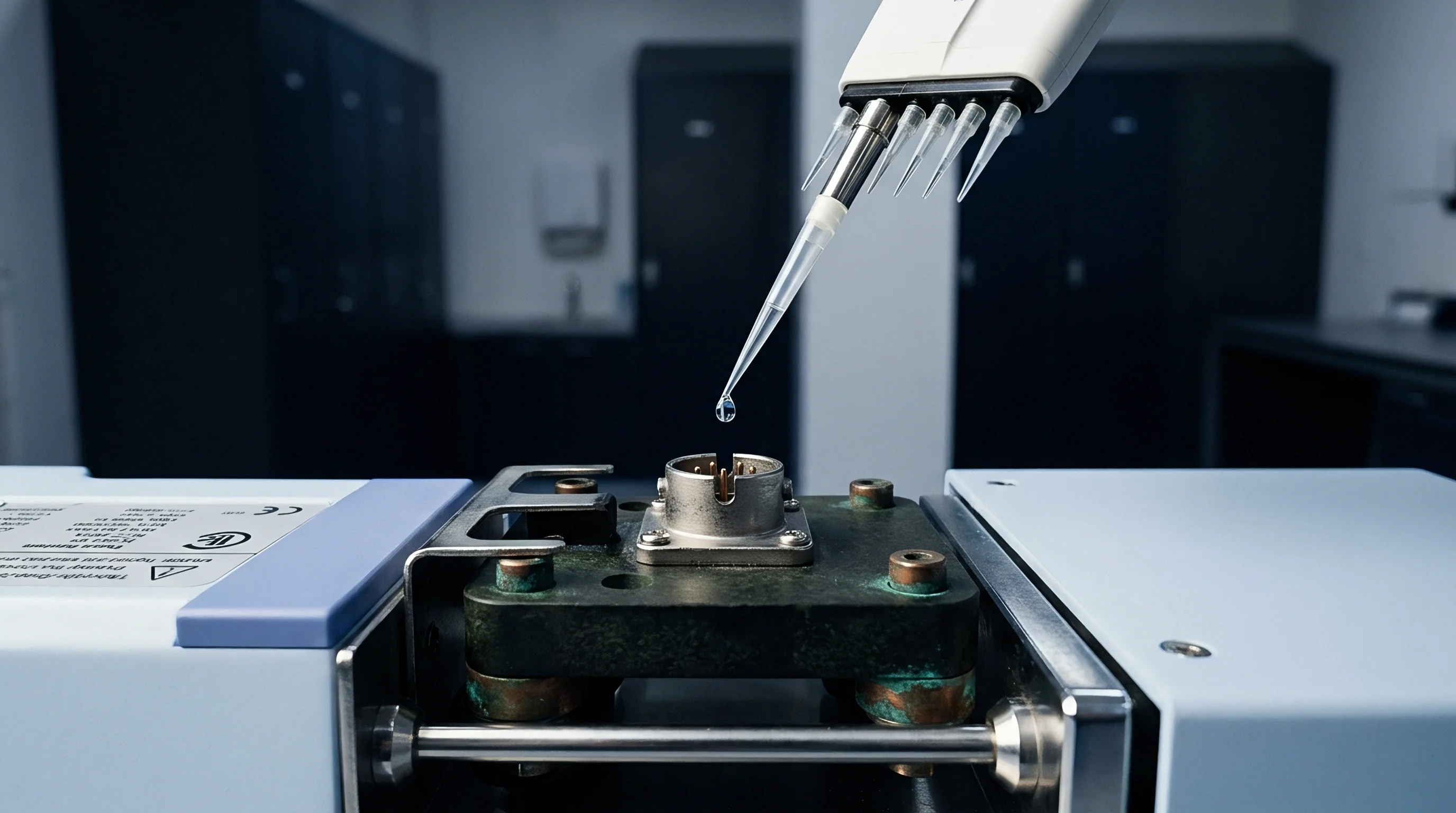
Silicon Pedestal Mounts and Stress Relief Cutouts
Interposing a glass or silicon spacer between the sensor element and ceramic cavity reduces direct strain transmission. Pyrex 7740 glass spacers closely match the thermal expansion coefficient of single-crystal silicon. Elevating the active micromachined die away from the ceramic floor on an intermediate glass pedestal allows shear forces from adhesive mismatch to dissipate within the glass volume before reaching sensitive comb structures.
Glass-to-silicon anodic bonding creates a rigid, void-free hermetic joint with minimal residual mechanical strain. Machining stress-relief slots or perimeter isolation trenches into the silicon substrate shields central anchor points from outer die margin warpage. Suspension anchors anchored exclusively to a central pedestal footprint experience negligible strain when outer margins flex, whereas suspension systems attached near outer perimeters absorb maximum warpage and suffer higher thermal bias drift.
Compliance Mitigation in Module Level Enclosures
Modular sensor assemblies rely on soft potting gels and floating mechanical frames to block external board bending moments. Encapsulating high-precision accelerometers in ultra-soft silicone gel isolates package housings from external forces; because silicone gels have very low elastic moduli, they absorb shock and expansion differentials without transmitting significant static stress to internal ceramic substrates.
Structural isolation extends to board-level integration through compliant lead frames or flexible substrate cutouts. Machining perimeter routing slots around the sensor footprint on the circuit board creates a suspended mounting tab supported by narrow neck bridges. Board flexure caused by thermal expansion or enclosure mounting bolts deforms these flexible necks, blocking structural strain before it reaches the accelerometer carrier.
| Isolation Method | Attenuated Stress Vector | Attenuating Mechanism | Mechanical Drawback | Target Stability Level |
|---|---|---|---|---|
| Anodically Bonded Glass Pedestal | In-plane die-attach shear | Volumetric strain dissipation | Increased total package height | Sub-100 micro-g bias drift |
| Central Single-Anchor Mounting | Out-of-plane die bending | Symmetrical radial expansion | Lower rotational shock tolerance | Sub-500 micro-g bias drift |
| Silicon Substrate Stress Cutouts | Perimeter mounting warpage | Compliant mechanical flexures | Increased total die surface area | Sub-1 mg bias drift |
| Compliant Silicone Gel Encapsulation | External chassis deflection | Ultra-low modulus buffer | Potential outgassing concerns | Sub-2 mg bias drift |
| PCB Suspended Mounting Tabs | Circuit board mechanical flexure | Flexible neck tab flexures | Reduced high-frequency response | Sub-5 mg bias drift |
Integrating isolation mechanisms requires systematically selecting materials, structural geometries, and mounting methods based on critical sensor requirements.
- Match pedestal thermal expansion to silicon substrate values using borosilicate glass or single-crystal silicon spacers to minimize interface strain.
- Position sensing anchor points centrally on the pedestal footprint to leverage radial expansion symmetry and cancel differential stress vectors.
- Implement perimeter stress relief slots around active micro-machined areas to isolate suspension anchors from die-edge mechanical warpage.
- Select low-modulus die attach materials with glass transition temperatures well outside operational thermal boundaries to prevent modulus steps.
- Design suspended circuit board mounting tabs with flexible neck bridges to decouple board bending loads from sensor package leads.
Combining wafer-level capping with MIL-STD-883 Method 1010 condition B preconditioning in incoming supply contracts ensures thermal stress degradation manifests prior to module integration.


Arbitration
Commercial datasheets often obscure stress-induced drift by highlighting room-temperature noise figures while omitting wide-band thermal drift limits. Sourcing high-precision accelerometers requires qualification protocols that expose thermomechanical stress vulnerabilities before committing to volume production. System integrators establish rigorous verification procedures, screening criteria, and contractual terms to ensure sensor performance holds across real-world thermal environments.
Standard component-level qualifications frequently miss assembly-level thermal stress transfer. A sensor component that demonstrates excellent thermal stability on an unconstrained test socket can exhibit severe zero-g offset drift once soldered to a thick multi-layer circuit board and mounted inside an aluminum chassis. Verification must evaluate the fully integrated assembly under realistic thermal gradients and boundary conditions.

Qualification Standards and Environmental Chamber Testing
Verifying sensor stability under operational thermal gradients requires specialized test profiles with controlled dwell times and ramp rates. Standard environmental stress screening protocols, such as AEC-Q100 Grade 1 or MIL-STD-883 Method 1010, cycle components between -40°C and +125°C. However, evaluating thermal stress transfer in precision accelerometers demands continuous sensor power and data logging throughout the entire chamber cycle.
Static soak measurements at fixed temperature steps fail to capture dynamic gradient effects. Applying rapid thermal ramps (e.g. 5°C per minute) exposes offset spikes driven by transient temperature differences across internal package materials.
Plotting sensor output against temperature during continuous cycling reveals the thermal hysteresis loop area, offering a direct metric of viscoelastic creep and micro-yielding within internal package interfaces.

Sourcing Risk Management across Assembly Supply Chains
Evaluating wafer foundries and packaging vendors requires examining material control consistency alongside thermal hysteresis guarantees. Slight variations in die-attach epoxy thickness or cure percentage dramatically alter thermal stress transfer across production lots. Consequently, procurement contracts for precision applications must specify strict process control limits for die-attach bondline thickness, tilt, and fillet height uniformity.
Dual-sourcing sensor components introduces integration risks if alternate suppliers use different internal packaging architectures. A primary source using a glass pedestal mount exhibits drastically different thermal stress performance compared to a second-source vendor using direct silver-epoxy die attach inside an identical ceramic footprint. Substituting components based solely on external footprint compatibility risks catastrophic bias drift failures in the field.
Evaluating thermal stress performance in incoming sensor shipments requires a structured testing sequence to isolate assembly-induced strain errors.
- Mount sample sensors onto standardized baseline evaluation test boards using defined reflow thermal profiles.
- Perform an initial 24-hour thermal stabilization soak at 25°C to record baseline zero-g offset and scale factor values.
- Subject mounted assemblies to five complete thermal cycles from -40°C to +125°C with a controlled ramp rate of 2°C per minute.
- Log accelerometer offset outputs continuously during ramps and 30-minute dwell periods at thermal extremes.
- Calculate total thermal hysteresis loop area and maximum transient gradient bias error across the complete cycle.
- Reject component lots whose maximum hysteresis offset shift exceeds the specified system error budget threshold.
Whether sub-micro-g bias stability can be achieved in mold-compound plastic QFN packages without ceramic carriers remains an open question for next-generation inertial sensing applications.