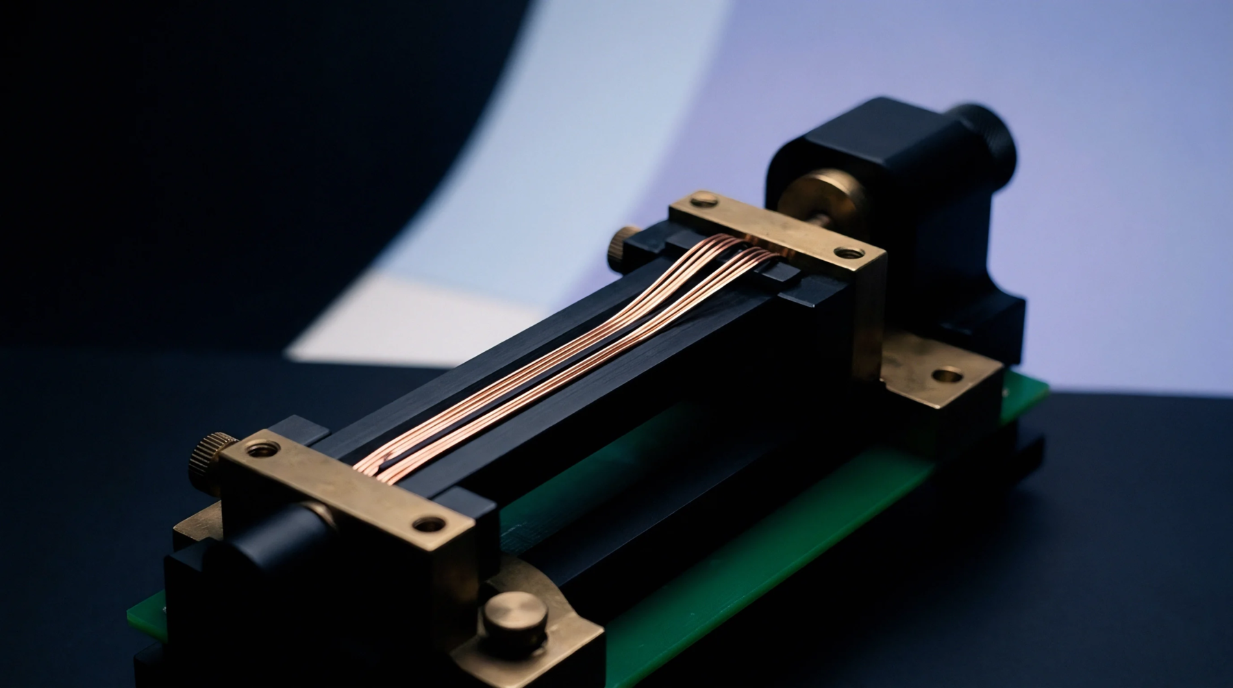
High Volume Probe
The quality screening procedure assesses the electrical performance and physical health of individual sensor dies while they remain attached to the large circular substrate. During wafer level testing, a probe station uses needles to contact microscopic bond pads to drive signals and measure identical site responses. This early identification ensures that only healthy units proceed into the final packaging steps which saves significant assembly time and component material resources.
The screening stops at simple functional checks before specialized environmental testing occurs later in the production line using individual packages. It measures output variables against design targets to identify spatial patterns of defects that point toward specific manufacturing equipment failures. Certificates from this process record yield statistics and electrical map data that guide the final dicing and selection sequence.
Defect Localization
Patterns of failure across the disc help engineers isolate systematic errors from process drift during thermal or chemical steps in the cleanroom. While utilizing wafer level testing, map software creates color coded diagrams showing which zones contain higher counts of resistive or capacitive deviations. This shift toward spatial data allows for faster maintenance of tools like developers or ion implanters when signatures of failure appear repeatedly.
Drift in probe alignment can damage pad surfaces and create false negatives where good silicon appears broken due to poor contact force. Calibration of the probing mechanism involves checking contact resistance against a gold plated master site to verify the tips are clean and firm. Installation of test programs requires periodic verification with a control wafer to ensure consistency in detection sensitivity throughout every work week.
Precision Verification
Testing thousands of potential microchips in a single hour requires sophisticated timing controls and stable low noise electronic pathways into the handler. Measuring accuracy from precision probe sweeps depends on minimizing electromagnetic noise in the cable bundle between the tester and the load board. Interference from stray signals at high frequency can mask subtle non linearities in the sensor bridge that would emerge as errors later on.
Tolerance for signal limits is set narrow at this stage to build a margin of safety for potential drift during final assembly steps. Specification at reference conditions marks the zero bias and span output limits that every die must satisfy to leave the fab cleanroom. Technicians monitor the contact life of the needles to ensure that mechanical fatigue does not introduce variable resistance into the sensor path.
Process Efficiency
Screening early provides the main protection against shipping batches with latent failures that might only trigger under environmental loading conditions in the field. When performing wafer level testing, testers confirm that basic properties like ohmic isolation and bridge balance meet the standard quality specifications for the device. The measurement it attests forms the basis for the final quality report issued for every completed silicon lot in the inventory system.
Beyond the physical limits of the bond pad, probing becomes impossible which limits the check to items that have functional electrical access points. Final verification ensures that calibration maps stay linked correctly to the unique location coordinates of every single chip throughout the entire manufacturing journey. Accurate mapping saves material costs by rejecting faulty silicon immediately.