Thermal Hysteresis and Dynamic Mechanical Strain in Accelerometer Zero Offset Determinations
Thermal hysteresis and package strain corrupt accelerometer zero offset; accurate baseline determinations require thermal soak isolation and vibration rejection.


Transduction

Zero Offset Physics in Inertial Sensing
Zero-g offset is the electrical output of an accelerometer when no external acceleration acts along its sensitive axis. Acceleration transducers rely on mechanical proof masses suspended by flexures, where displacement or stress translates into capacitance change, resistance variation, or piezoelectric charge generation. In an ideal transducer, the resting output corresponds to a predictable factory-calibrated baseline.
Environmental fields disrupt this resting state through non-acceleration inputs. Temperature shifts alter element geometry, the Young’s modulus of silicon or quartz suspension beams, and internal stress distributions. Dynamic mechanical forces transmitted through mounting structures introduce instantaneous flexure that the sensing element misinterprets as kinematic translational motion.
Determining an accurate zero-g offset requires separating true structural acceleration from environmental strain fields acting on the transducer package.
Precision inertial systems require bias stability measured in micro-gravitational units over extended operational windows. Marine navigation, tilt monitoring on civil structures, and borehole survey toolsets operate where a baseline shift translates directly into cumulative positional drift or angular error. When zero offset calibration occurs on a static bench, the recorded bias reflects the equilibrium state of that specific fixture at that exact temperature.
Operating environments rarely mirror bench conditions. Temperature gradients cause non-uniform thermal expansion across the die, package, and substrate, while thermal cycling triggers micro-structural yielding in die-attach adhesives and wire bond interfaces. High-frequency structural vibration generates dynamic strain that propagates through the housing, shifting the proof mass’s resting position through non-linear elastic mechanics.
The baseline captured during factory calibration breaks down once these physical mechanisms alter the mechanical zero state of the sensing core.
Capacitive MEMS structures dominate high-volume precision applications, using micro-machined silicon combs where differential capacitance measures mass displacement. The mechanical stiffness of single-crystal silicon displays a temperature coefficient of Young’s modulus near minus sixty parts per million per Kelvin. As ambient temperature changes, suspension stiffness varies, shifting the proof mass position under residual internal stress fields.
Piezoresistive accelerometers use micro-machined silicon beams embedded with doped piezoresistors, translating strain directly into resistance variation across a sensing bridge. Thermally induced stress in piezoresistive layouts alters resistor values independently of mass motion, causing thermal offset drift. Piezoelectric devices generate charge through crystalline lattice distortion under dynamic loads, providing high mechanical bandwidth while naturally filtering static baseline measurements.
Each transduction modality introduces its own thermal and mechanical sensitivities into the primary acceleration signal path.
Quantifying offset stability requires evaluating the transducer, the mechanical interface, and the signal conditioning chain as an integrated system. Analog front-end electronics contribute thermal drift through op-amp input bias currents, voltage reference drift, and switch resistance changes in switched-capacitor readout circuits. Differential topologies mitigate symmetric electrical drift, leaving mechanical element asymmetry as the main driver of baseline instability.
This mechanical asymmetry stems from manufacturing tolerances in silicon etching, non-uniform film deposition, and anisotropic thermal expansion across multi-material chip assemblies. When external dynamic strain or thermal cycling acts on an asymmetric structure, the resulting differential force alters the zero offset independently of external kinematic acceleration.
The static zero-g offset recorded on a thermal equilibrium bench fails to predict operational bias stability when housing strain and cyclic temperature excursions alter internal package stress distributions.

Thermomechanical Stress Transmission Pathways
Silicon sensing dies reside within protective packages constructed from ceramic, metal, or molded plastic. The coefficient of thermal expansion mismatch between single-crystal silicon, ceramic substrates, organic die-attach adhesives, and copper leadframes creates localized stress concentrations during ambient temperature transitions. Eutectic gold-tin preforms or silver-filled epoxy layers bond the silicon die to the substrate cavity.
As the package cools from high-temperature assembly to room temperature, differential shrinkage leaves locked-in compressive strain across the die plane. Subsequent environmental temperature swings alter this strain state, causing the package floor to bow or twist. Because the sensing element anchors directly to the die plane, substrate flexure transfers displacement strain into the suspension flexures holding the proof mass.
The geometry of the anchor points dictates how die-plane strain reaches the micro-machined suspension. Center-anchor topologies mount the proof mass and frame to the die substrate at a single central point, allowing surrounding silicon to expand or contract symmetrically without transferring package-level thermal strain into the active flexures. Ring anchors or multi-point perimeter anchors pin the sensing structure at multiple coordinates across the die plane.
Axisymmetric perimeter anchors convert sub-micron package distortions directly into mechanical beam deflection, producing large baseline offsets. Temperature ramps induce spatial thermal gradients across the package enclosure when heating rates outpace internal thermal diffusion. Differential expansion between the top lid and bottom substrate generates transient thermomechanical bending moments that distort perimeter-anchored sensing dies long before isothermal equilibrium is re-established.
Polymeric die-attach materials introduce viscoelastic behavior that compounds thermal stress transmission. Epoxies display temperature-dependent storage moduli and loss tangents, shifting dramatically near their glass transition temperature. Below this region, the adhesive acts as a rigid glass, transmitting substrate expansion strain directly into the silicon die.
Above the glass transition temperature, the material softens into a rubbery state, relaxing structural strain but increasing susceptibility to mechanical creep under sustained external loads. During temperature ramps, the transition between these regimes causes non-linear offset shifts that cannot be corrected with simple first-order or second-order polynomial temperature coefficients.
Substrate flexure from host printed circuit board mounting introduces an external strain channel that couples directly into the internal thermomechanical stress pathway. Soldering a ceramic or plastic accelerometer package onto an FR4 circuit board introduces a substantial thermal expansion mismatch. FR4 exhibits an in-plane thermal expansion coefficient near fourteen to seventeen parts per million per Kelvin, whereas alumina ceramic sits near six to seven parts per million per Kelvin, and silicon sits near two point six parts per million per Kelvin.
Reflow soldering locks high residual shear stresses into the solder joint pads at the alloy’s solidification temperature. Environmental temperature changes cause the host circuit board to push and pull against the package pads, bending the package substrate and shifting the baseline transducer offset. Failing to isolate the package from host board strain degrades zero offset repeatability across operational temperature limits, leading to inaccurate calibration routines and unexpected bias errors in the field.


Bond

Thermal Hysteresis Mechanisms in Package Assemblies
Thermal hysteresis manifests as a non-repeatable zero-g offset value when an accelerometer returns to a reference temperature following an excursion to a temperature extreme. The baseline offset recorded at twenty-five degrees Celsius prior to thermal cycling differs from the offset measured at twenty-five degrees Celsius after cooling to minus forty degrees Celsius or heating to one hundred twenty-five degrees Celsius. This deviation corrupts long-term bias tracking because the zero offset becomes a path-dependent parameter rather than a single-valued function of instantaneous temperature.
Thermal hysteresis arises from micro-structural damage, stress relaxation, viscoelastic relaxation, and moisture desorption-adsorption within the multi-material package stackup.
Viscoelastic creep in die-attach epoxies is a primary driver of zero offset thermal hysteresis. When the assembly sits at elevated temperatures under locked-in thermomechanical strain, polymeric chains within the die-attach adhesive slowly reorient to relieve internal shear stress. This relaxation reduces the compressive force exerted on the silicon die at high temperatures.
Upon returning to room temperature, the relaxed polymer prevents the die from returning to its original stress state, leaving a permanent residual stress delta. The magnitude of this delta depends on peak exposure temperature, dwell time, cooling rate, and the mechanical stress history of the adhesive layer. Polymeric creep kinetics follow non-linear time-temperature superposition principles, generating variable hysteresis loops across different operational thermal profiles.
Micro-yielding and grain boundary sliding in metallic bond materials create permanent offset steps following thermal cycling. High-performance accelerometers using gold-silicon eutectic or gold-tin solder die-attach interfaces avoid polymer viscoelasticity, but remain vulnerable to metallic plastic deformation. Thermal expansion mismatch between the silicon die and the package cavity generates shear stresses that exceed the yield strength of soft solder alloys at elevated operating temperatures.
Microscopic plastic slip along metallic grain boundaries redistributes internal strain across the bottom die surface. When the transducer returns to ambient conditions, the permanently deformed metallic lattice holds the silicon frame in an altered geometric state, permanently shifting the capacitive comb alignment or piezoresistive bridge balance point.
Moisture absorption inside plastic encapsulated microcircuit packages alters internal strain fields through hygroscopic swelling. Mold compounds and die-attach polymers absorb ambient atmospheric moisture during storage and operation. Absorbed water molecules disrupt hydrogen bonding between polymer chains, lowering the material’s glass transition temperature and inducing volumetric expansion.
When the accelerometer encounters elevated temperatures during operation or testing, absorbed moisture rapidly desorbs from the package layers. This volumetric shrinkage changes the mechanical stress applied to the embedded silicon die independently of pure thermal expansion. Outgassing and moisture exchange create offset hysteresis loops that depend heavily on ambient relative humidity and preconditioning history.
A ceramic package exhibiting two milligrams of thermal offset hysteresis across a sixty-degree cycle introduces an uncompensated navigation position error that scales quadratically with operational duration.

Dynamic Mechanical Strain Rectification
Dynamic mechanical strain refers to time-varying mechanical flexure imposed upon the sensor package by structural vibration, acoustic excitation, or high-frequency structural bending. While linear acceleration components within the sensor passband register as valid signals, out-of-band dynamic strain can distort the static zero offset through mechanical and electrical non-linearities. Vibration Rectification Error (VRE) occurs when alternating dynamic acceleration or mounting strain generates a net shift in the average DC baseline signal.
High-frequency structural resonances in the sensor housing or host circuit board amplify incoming dynamic strain, driving the sensing element into non-linear regimes where symmetric oscillatory motion converts directly into static zero offset drift.
Structural non-linearities in micro-machined silicon flexures drive mechanical rectification. Micro-machined capacitive comb fingers use squeeze-film air damping or rarefied gas damping to control frequency response near resonance. Squeeze-film damping forces are inherently non-linear with displacement: as the gap between moving and stationary comb fingers closes, fluidic damping forces increase exponentially compared to when the gap opens.
Under high-amplitude vibration, this asymmetric damping force prevents symmetrical oscillation of the proof mass about its neutral axis. The time-averaged position of the proof mass shifts away from mechanical zero, creating a false DC acceleration output that persists for the duration of the mechanical disturbance.
Electrostatic non-linearities in closed-loop and open-loop capacitive readout topologies further compound strain rectification. The electrostatic force between parallel capacitive plates varies inversely with the square of the inter-plate distance. When dynamic mechanical strain flexes the sensor housing, shifting stationary stator plates relative to the moveable rotor assembly, the instantaneous electrostatic restoring force becomes highly asymmetric over the vibration cycle.
In closed-loop accelerometers using pulse-density or pulse-width modulation force-rebalance feedback, severe dynamic strain inputs can momentarily saturate feedback driver electronics. Feedback saturation collapses the electrostatic hold on the proof mass, causing large baseline offset spikes and persistent zero-g recovery tails after the dynamic strain subsides.
Acoustic strain coupling presents a non-contact pathway for baseline offset corruption. High-intensity acoustic energy from machinery, propulsion units, or airflow turbulence flexes thin package lids and ceramic cavity substrates at kilohertz frequencies. If an acoustic excitation frequency aligns with an internal structural resonance of the MEMS frame or an undamped substrate bending mode, local strain amplitudes scale dramatically.
Dynamic acoustic strain flexes the die substrate, modulates inter-element capacitance, and shifts the zero-g offset through squeeze-film non-linearities and amplifier slewing limits. Transducers operating in intense acoustic fields require hermetic, thick-walled housing architectures or acoustic isolation barriers to prevent acoustic strain rectification from corrupting static tilt or low-frequency measurements.
| Material Application Layer | Material Composition Type | CTE Value Range (ppm/K) | Elastic Modulus (GPa) | Glass Transition Tg (C) | Hysteresis Susceptibility |
|---|---|---|---|---|---|
| Sensing Core Die | Single-Crystal Silicon | 2.6 | 130 – 169 | Not Applicable | Baseline Reference |
| Die Attach Adhesive | Silver-Filled Epoxy | 30 – 65 | 3 – 8 | 60 – 150 | High (Viscoelastic Creep) |
| Die Attach Preform | Eutectic Gold-Tin (80/20) | 16.0 | 59 | Not Applicable | Low (Micro-Yielding) |
| Hermetic Substrate | Alumina Ceramic (96% Al2O3) | 6.5 – 7.2 | 300 | Not Applicable | Very Low (Brittle Elastic) |
| Plastic Encapsulant | Epoxy Molding Compound | 10 – 16 | 15 – 25 | 120 – 175 | High (Hygroscopic & Creep) |
| Host Circuit Board | Standard FR4 Laminate | 14 – 17 | 18 – 22 | 130 – 170 | Moderate (Board Flexure) |
Mitigating thermomechanical instability requires careful packaging selection and board layout geometry. Engineers must recognize the physical failure modes that introduce unexpected baseline steps during operational qualification testing.
- Die-attach stress relaxation alters the residual compressive strain on silicon anchor points following high-temperature dwells, creating persistent zero-g offset shifts.
- Solder joint creep fatigue under leadless chip carrier packages degrades constraint symmetry across the package perimeter, inducing thermal-cycle offset hysteresis.
- Squeeze-film damping asymmetry rectifies high-frequency out-of-band structural vibration into false low-frequency DC acceleration offsets inside the signal conditioning path.
- Substrate glass transition shifting in organic encapsulants releases locked-in assembly forces during thermal ramps, corrupting first-order temperature compensation models.
- Acoustic flexure coupling through thin package lids flexes internal comb stators at acoustic resonant frequencies, generating vibration rectification error.
Sourcing engineers evaluating high-precision accelerometers frequently encounter supplier claims asserting zero thermal hysteresis across wide operational temperature ranges. Vendors achieve these claims on datasheets by standardizing slow thermal ramp rates during factory acceptance testing, allowing viscoelastic stresses to relax continuously without building measurable thermal lag. When the same transducer experiences rapid thermal shock in a field deployment, unrelaxed internal shear forces induce significant baseline hysteresis steps.
Standard factory screening routines simply mask the underlying mechanical vulnerability inherent to the vendor’s die-attach chemistry.


Rectification

Dynamic Vibration Rectification Modeling
Vibration Rectification Error converts alternating peak-to-peak acceleration or dynamic structural strain into an equivalent static baseline shift. Mathematically, VRE is defined as the change in average DC output when a sinusoidal or random vibration field acts on the accelerometer along a specified axis. The rectification coefficient, expressed in units of acceleration shift per acceleration squared, quantifies this susceptibility.
When an accelerometer experiences dynamic inputs above its mechanical bandpass, non-linear transfer functions within the transducer generate second-order intermodulation products. The second-order term of a Taylor series expansion modeling the force-to-displacement characteristic yields a constant DC offset term proportional to the square of the input dynamic amplitude.
In a capacitive micro-machined accelerometer subject to single-frequency dynamic acceleration, proof-mass displacement involves both linear compliance and higher-order stiffness from beam suspension stretching. Once proof mass displacement exceeds a small percentage of the capacitive gap, the mechanical restoring force from the suspension flexures grows asymmetrical, becoming stiffer in one direction than the other. Integrating this non-linear displacement over complete vibration cycles produces a net non-zero time-averaged displacement.
The capacitive sense amplifier processes this non-zero mean displacement as a continuous zero offset drift, indistinguishable from true static acceleration.
Readout amplifier slewing limits and Phase-Locked Loop demodulation dynamics contribute an additional electronic pathway for dynamic strain rectification. Analog front-end amplifiers possess finite slew rates and upper dynamic range limits. High-frequency dynamic strain induced by mechanical resonance generates large peak-to-peak voltage oscillations at the preamplifier input node.
If the peak voltage slew rate exceeds the amplifier’s maximum slew rate, the output waveform becomes asymmetric, clipping positive or negative peaks. Passing a clipped, asymmetric waveform through an integrated low-pass reconstruction filter produces a non-zero DC bias shift. Electronic rectification can occur even if the mechanical sensing die operates entirely within its linear elastic regime, underscoring the need to evaluate the complete signal chain under dynamic mechanical excitation.
Random vibration environments present broad spectrum power spectral densities that excite multiple housing, board, and sensor resonances simultaneously. Multi-axis dynamic strain inputs cause cross-axis coupling, where dynamic flexure orthogonal to the primary sensitive axis modulates the gap width along the sensitive axis. Cross-axis strain coupling coefficients scale with internal mechanical misalignment and package mounting non-planarity.
In tactical navigation and industrial monitoring, random vibration fields frequently generate zero offset shifts ranging from several hundred micro-gravitational units up to tens of milligram units, corrupting integrated velocity and position calculations.
Under international calibration standard ISO 16063-16, zero offset stability under dynamic vibration must be reported as a VRE coefficient in milligrams per g-squared across specified octave frequency bands.
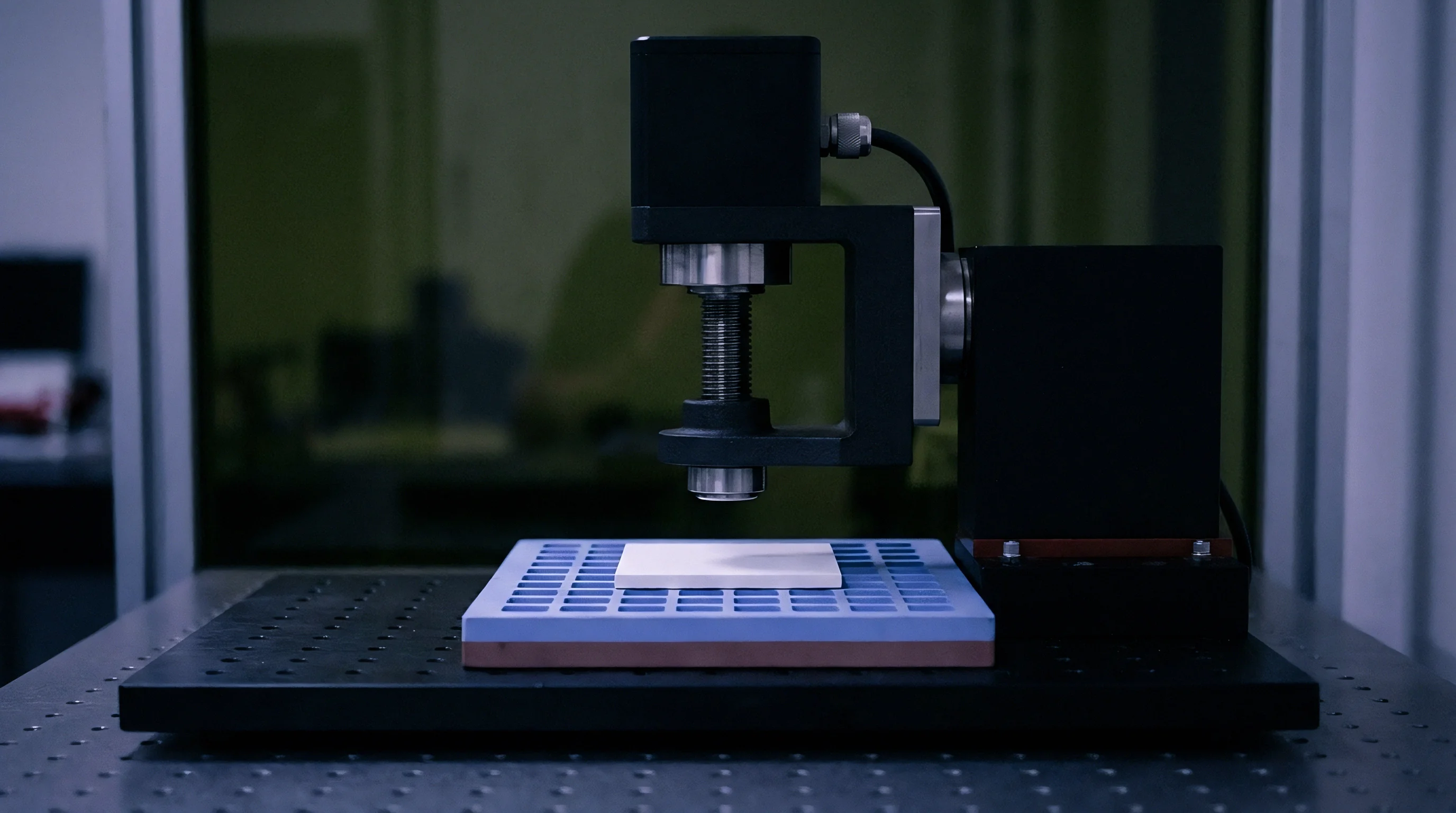
Dynamic Mechanical Strain Isolation Architectures
Isolating the sensitive element from dynamic mechanical strain requires structural decoupling between the host printed circuit board and the internal MEMS die. Package-level decoupling strategies employ compliant mechanical mounts, stress-isolation slots cut into host circuit boards, and dedicated micro-machined interposers. A silicon micro-machined interposer sits between the active sensing die and the ceramic package substrate, using micromachined flexures to absorb substrate thermal expansion and dynamic flexure strain.
The interposer acts as a mechanical low-pass filter, transmitting static acceleration signals while attenuating high-frequency mechanical strain waves before they reach the sensitive comb structures.
Board layout geometry directly dictates the amplitude of dynamic flexure strain transmitted to the sensor pins. Mounting an accelerometer in the center of a large, unstiffened printed circuit board exposes the package to maximum bending moments during board vibration modes. Bending moments compress top-side surface-mount component pads and stretch bottom-side pads, imparting severe cyclic shear stresses to corner solder joints.
Positioning the accelerometer adjacent to mechanical board supports, card-edge stiffeners, or rigid mounting standoffs minimizes dynamic flexure. Perimeter strain-relief slots, routed through the circuit board dielectric around three sides of the package footprint, create a compliant mechanical peninsula that attenuates board flexure forces by over twenty decibels.
Mechanical mounting torque applied during assembly represents a major source of initial static stress and dynamic strain amplification. Fastening a rigid accelerometer package or aluminum module housing onto a non-flat mounting surface induces severe frame warping. As mounting screws tighten against an uneven surface, the metallic or ceramic housing flexes to conform to the surface topology.
This assembly strain flexes the internal die cavity, shifting the zero offset baseline immediately upon torque application. Thermal cycling under high mounting stress accelerates bolt relaxation and interface settling, introducing persistent offset drift over operational lifetimes. Using three-point kinematic mounts or precision ground interface surfaces prevents mounting torque strain from distorting the internal transducer core.
Viscoelastic damping materials placed beneath component packages offer secondary attenuation against acoustic and structural shock strain. Silicone potting compounds, soft elastomeric pads, and fluorosilicone underfills dissipate high-frequency acoustic wave energy before it penetrates the package lid. However, organic damping materials introduce temperature-dependent mechanical properties that alter system resonances across ambient thermal limits.
Underfill epoxies must be chosen with precise glass transition temperatures outside the operational range and thermal expansion coefficients matched to the solder ball arrays to avoid worsening thermal hysteresis while trying to mitigate mechanical strain rectification.
| Transduction Modality Type | VRE Coefficient (mg/g2) | Primary Rectification Pathway | Cross-Axis Strain Coupling | Acoustic Sensitivity |
|---|---|---|---|---|
| Open-Loop Capacitive MEMS | 0.5 – 5.0 | Squeeze-Film Damping Asymmetry | Moderate (0.5% – 2.0%) | High (Lid Flexure) |
| Closed-Loop Force-Rebalance | 0.01 – 0.1 | Feedback Driver Slew Clipping | Very Low (< 0.1%) | Low (Stiff Cavity) |
| Silicon Piezoresistive Bridge | 0.1 – 1.5 | Piezoresistive Piezojunction Shear | High (1.0% – 3.5%) | Moderate (Substrate Flex) |
| Quartz Flexure Accelerometer | 0.001 – 0.05 | Quartz Flexure Non-Linear Elasticity | Extremely Low (< 0.01%) | Very Low (Hermetic Metal) |
| Surface Acoustic Wave (SAW) | 2.0 – 12.0 | Direct Substrate Acoustic Mixing | High (Direct Substrate) | Extremely High |
Executing accurate zero offset determinations requires systematically applying a sequence of isolation steps during bench qualification and system integration testing.
- Mechanical surface flatening ensures the test fixture and sensor base exhibit surface non-planarity under five micrometers across the mounting footprint to prevent mounting strain warping.
- Torque-controlled fastening applies mounting screw tension in a calibrated star pattern using precision torque limiters to prevent localized package bending stresses.
- Thermal soak stabilization maintains the transducer package at the target qualification temperature for a duration exceeding three thermal time constants prior to recording baseline zero-g offset data.
- Spectral vibration auditing monitors out-of-band high-frequency structural vibration using a broad-band reference transducer to detect dynamic strain components capable of triggering vibration rectification error.
Where does high-frequency dynamic strain yield false zero offset shifts in systems operating under broad-spectrum acoustic noise?
When high-intensity acoustic fields excite structural housing modes, the ceramic substrate flexes at frequencies far exceeding the bandwidth of the analog readout filter. The mechanical comb structures experience intermodulation, translating acoustic pressure waves into continuous baseline DC drift. Pinpointing this pathway requires testing the isolated transducer in an acoustic chamber while maintaining zero kinematic acceleration inputs.
If zero-g baseline offset shifts correlate directly with acoustic Sound Pressure Level independently of physical shaker motion, acoustic lid flexing is the active corruption mechanism.


Chamber

Bench Isolation and Test Protocol Design
Accurate baseline zero offset determinations require thermal chamber testing designed to isolate true sensor thermal characteristics from fixture-induced mechanical strain and transient thermal gradients. Standard industrial environmental chambers use forced-air convection, which generates rapid spatial thermal turbulence and localized high-velocity air streams. Placing a bare circuit board directly in a forced-air stream induces dynamic spatial thermal gradients across the accelerometer package, driving transient thermomechanical bowing.
Convection-induced thermal gradients mask intrinsic steady-state zero-g offset profiles, yielding erratic temperature coefficients and false hysteresis measurements.
To eliminate air turbulence and spatial thermal gradients, bench qualification setups use heavy thermal copper or aluminum soak blocks enclosing the device under test. A high-mass aluminum soak block acts as a spatial low-pass thermal filter, smoothing ambient air fluctuations and ensuring uniform heat conduction into all sides of the sensor package simultaneously. The device under test attaches to the thermal block using thin, non-filled silicone grease interfaces or soft thermal graphite pads rather than rigid mechanical clamps.
Rigid mechanical clamping against a copper block forces thermal expansion mismatches between the metallic block and the host circuit board directly into the sensor pins, generating massive fixture-induced strain offsets during temperature ramps.
Thermal ramp rates during offset determination testing must be precisely controlled to separate transient thermomechanical strain from true isothermal equilibrium offset properties. Uncontrolled chamber ramps exceeding five degrees Celsius per minute generate large internal temperature differences between the external package lid and the internal silicon die. Differential expansion during rapid ramps causes transient substrate bowing, resulting in wide baseline offset hysteresis loops that vanish when the ramp rate slows.
Standardized qualification protocols mandate soak times at discrete temperature steps, maintaining temperature stability within plus or minus zero point one degree Celsius for minimum durations of thirty to sixty minutes per step. Isothermal step profiles allow internal material strain fields to reach complete equilibrium before recording baseline zero-g offset points.
Gravitational field vector alignment represents another critical variable during chamber zero offset determinations. Measuring true zero-g baseline offset requires orienting the sensitive axis precisely perpendicular to the Earth acceleration vector, or using a multi-position tumble test protocol. In a two-position tumble test, the accelerometer sensitive axis aligns parallel and anti-parallel to gravity, yielding plus one-g and minus one-g reading pairs.
Summing the two outputs and dividing by two cancels the true gravitational acceleration vector, isolating the static zero-g offset baseline. The mechanical tumble fixture inside the chamber must maintain precise angular positioning accuracy under one hundred arc-seconds across all temperature extremes to prevent gravitational vector bleed from masquerading as thermal offset drift.
A thermal qualification chamber operating without spatial low-pass soak blocks introduces air convection gradients that corrupt baseline offset repeatability measurements by several milligrams.

Decoupling Strain and Thermal Offsets
Separating dynamic mechanical strain offsets from pure thermal baseline drift requires systematic mathematical and physical signal decomposition. Mechanical strain applied to a sensor package modulates the zero offset independently of local temperature. However, ambient temperature changes simultaneously modify the mechanical properties of the package, coupling the two channels into a combined offset response.
Test engineers employ dual-mode sensing structures and external strain gauge instrumentation to measure package flexure directly during thermal calibration sweeps.
Resistive strain gauges mounted on the underside of the host circuit board directly adjacent to the accelerometer package record substrate flexure during thermal chamber cycling. By capturing micro-strain values simultaneously with accelerometer output and die temperature, analysts construct a multivariable regression model separating pure thermal offset coefficients from strain-induced offset coefficients. The measured zero offset baseline is modeled as a linear superposition of an isothermal temperature polynomial and a strain transfer matrix.
Correcting raw calibration data using measured PCB micro-strain isolates the intrinsic silicon core thermal sensitivity, revealing whether observed hysteresis steps stem from internal die-attach relaxation or external circuit board flexing.
Advanced silicon accelerometers integrate stress-sensing piezoresistors co-located on the same silicon substrate adjacent to the primary capacitive suspension anchors. These integrated stress sensors measure internal die stress directly, independent of proof mass displacement. When host board flexure or package thermal expansion flexes the silicon die, the stress-sensing bridge outputs a millivolt signal proportional to local megapascals of mechanical stress.
The onboard signal processing ASIC uses this real-time stress data to subtract strain-induced offset shifts dynamically before outputting the final acceleration value to the host system. Internal stress-sensing topologies achieve high baseline offset stability across aggressive board-bending environments.
Software-based dynamic strain rejection algorithms monitor the spectral content of incoming sensor signals to detect out-of-band dynamic energy capable of driving vibration rectification. High-rate oversampling front-ends sample transducer element displacement at megahertz frequencies before applying digital decimation and low-pass filtering. By processing signal peak-to-peak excursions at high bandwidth, digital signal processing algorithms detect non-linear displacement signatures indicative of squeeze-film asymmetry or amplifier slewing.
When dynamic strain rectification triggers an offset shift, the internal DSP flags signal invalidity or applies real-time non-linear correction factors derived from factory vibration profiling.
| Calibration Environment Method | Spatial Thermal Uniformity (C) | Fixture Strain Inducted (ue) | Residual Offset Uncertainty | Cycle Hysteresis Repeatability |
|---|---|---|---|---|
| Unshielded Forced-Air Chamber | +/- 2.5 | 150 – 450 | +/- 8.0 mg | Poor (> 5.0 mg shift) |
| High-Mass Conduction Soak Block | +/- 0.05 | < 25 | +/- 0.3 mg | Excellent (< 0.2 mg shift) |
| In-Situ Strain Monitored Fixture | +/- 0.1 | Monitored (Subtract) | +/- 0.1 mg | Superior (< 0.05 mg shift) |
| Kinematic 3-Point Floating Mount | +/- 0.2 | < 5 | +/- 0.05 mg | Near-Ideal Baseline Limit |
Standard qualification procedures require completing a structured checklist before certifying zero offset baseline calibration accuracy in production environments.
Inspect the thermal soak block mounting interface to verify non-constrained mechanical floating conditions.
Verify that thermal chamber ramp rates remain under one degree Celsius per minute during continuous thermal sweep cycles.
Calibrate the multi-position tumble fixture angular encoder accuracy to ensure perpendicular alignment relative to Earth gravity within fifty arc-seconds.
Measure host circuit board micro-strain using calibrated strain gauges to confirm that substrate flexure remains below twenty micro-strain across the entire test temperature range.
Standard supply contracts governing automotive and aerospace sensor procurement specify strict adherence to qualification testing standards. Under clause 8.4.2 of standard IEC 60068-2-14 Environmental Testing Protocols, zero-g baseline offset measurements must be taken after maintaining the device under test at thermal equilibrium for a minimum of thirty minutes at each temperature step. Acceptance criteria specify that residual zero offset hysteresis following five consecutive thermal cycles between minus forty degrees Celsius and one hundred twenty-five degrees Celsius cannot exceed zero point five percent of the full-scale sensor measurement range.
Devices failing this threshold face lot rejection due to unrelaxed packaging stresses or substandard die-attach voiding ratios.


Contract

Datasheet Oversights and Sourcing Realities
Commercial sensor datasheets routinely obscure thermal hysteresis and dynamic strain performance through selective specification framing. Manufacturers prominently quote “Temperature Coefficient of Offset” (TCO) as a single linear or quadratic figure in milligrams per Kelvin or micro-gravitational units per Kelvin. This scalar parameter implies that zero offset drift is completely deterministic, reversible, and easily corrected using a simple polynomial lookup table in host firmware.
Datasheets rarely include thermal hysteresis specifications, concealing the fact that room-temperature zero offset shifts unpredictably after temperature cycles. A buyer specifying a component based solely on scalar TCO figures will discover uncompensated offset errors in the field that exceed the overall system error budget by orders of magnitude.
Vibration Rectification Error coefficients are similarly omitted from standard commercial sensor datasheets. Manufacturer testing typically occurs on ultra-quiet marble optical tables inside temperature-controlled cleanrooms. These pristine bench conditions eliminate out-of-band dynamic mechanical strain and acoustic energy.
In real-world applications ~ such as industrial pump monitoring, drone flight control, or automotive chassis systems ~ structural vibration and acoustic noise dominate the physical environment. An accelerometer displaying exceptional static zero offset stability on a marble bench can suffer catastrophic baseline shifts exceeding tens of milligrams when mounted on a vibrating structural frame, rendering host orientation algorithms entirely non-functional.
The gap between laboratory conditions and real-world PCB assembly mechanics creates substantial commercial friction between sensor buyers and primary wafer foundries. Wafer foundries test accelerometer dies at the bare silicon or wafer-level scale using flying probe pin interfaces. Bare die testing eliminates solder reflow thermal shock, die-attach cure stress, and FR4 substrate bending.
The foundry delivers fully functional silicon meeting strict offset drift limits on the wafer test report. Once the distributor packages the die and the tier-one contract manufacturer solders the component onto a host circuit board, thermal reflow stresses shift the baseline offset dramatically. Supplier warranties explicitly disclaim zero offset drift caused by customer board reflow processes, leaving the procurement engineering team responsible for absorbing yield loss or implementing costly post-assembly recalibration routines.
Dual-sourcing strategies introduce additional technical risk when baseline offset hysteresis varies between alternate wafer foundries or packaging vendors. An engineering team may qualify a primary supply source using a ceramic hermetic LCC package with eutectic gold-tin die attach, demonstrating minimal thermal hysteresis. To mitigate supply chain shortages, procurement cross-qualifies a secondary source providing a pin-compatible part in a plastic molded leadframe package using silver-filled epoxy.
While both components pass basic room-temperature functional screening and meet identical static acceleration range parameters, the plastic secondary source exhibits substantial viscoelastic creep, moisture swelling, and dynamic vibration rectification. Deploying the secondary part without updating firmware compensation algorithms introduces widespread operational field failures under thermal cycling environments.

Procurement Verification and Acceptance Standards
Establishing robust procurement specifications requires replacing generic datasheet metrics with explicit, testable baseline offset limits defined under realistic operational conditions. Sourcing engineering teams must draft custom Component Procurement Specifications (CPS) that mandate explicit maximum limits for thermal offset hysteresis, vibration rectification error, and mounting strain sensitivity. Procured components must undergo rigorous Lot Acceptance Testing (LAT) on incoming batches using specialized thermal-mechanical test fixtures before release to manufacturing lines.
Procurement contracts must stipulate acceptable limits for die-attach voiding verified via Acoustic Microscopy (C-SAM). Die-attach voids disrupt uniform thermal and stress transmission pathways across the bottom silicon surface. A localized void causes thermal expansion gradients that dramatically increase thermal hysteresis and spatial stress sensitivity.
Specifying a maximum allowable total voiding area below five percent of the die footprint, with no single void exceeding one percent under critical anchor points, ensures consistent mechanical stress coupling across production lots and reduces baseline offset variance.
Incoming inspection protocols must incorporate thermal shock screening designed to force early stress relaxation in unstable package assemblies. A sample from each incoming wafer lot undergoes ten rapid thermal shock cycles between environmental extremes with transfer times under ten seconds. Measuring the baseline zero-g offset before and after thermal shock screening isolates assemblies prone to high viscoelastic creep or micro-yielding.
Batches exceeding specified post-shock baseline hysteresis thresholds are returned to the vendor for credit, preventing unstable components from entering production streams and corrupting finished product quality.
Contractual guarantees regarding long-term zero offset drift must specify aging conditions, supply voltage fluctuations, and continuous mechanical stress levels. Long-term baseline stability specifications quoted as “typical zero drift over ten years” are legally unenforceable without specified operational duty cycles and environmental acceleration factors. Standardized purchasing agreements reference qualification standards such as AEC-Q100 Grade 0 or AEC-Q103-001 for automotive MEMS sensors, requiring explicit stress testing including High-Temperature Operating Life (HTOL), Temperature Cycling (TC), and Unbiased HAST (Highly Accelerated Stress Test).
Enforcing these standards transfers the financial and technical burden of zero offset verification back to the sensor manufacturer, protecting the buyer against undisclosed material substitutions or process degradation.
A reliable rule of thumb for sensor procurement dictates that any quoted zero offset stability parameter missing explicit ramp rate, soak time, and PCB mounting constraints must be treated as a bare die physical limit rather than a usable assembled component specification.