Measuring Temperature Coefficient of Offset in Capacitive MEMS Accelerometers
Measuring accelerometer offset drift requires thermal soak stabilization and multi-position gravity inversion to decouple mechanical stress from true bias shift.


Gradient
Thermal zero-point instability in a differential capacitive micro-electro-mechanical accelerometer originates from structural asymmetry under temperature flux. The proof mass suspends between fixed electrode fingers via folded micromachined silicon tethers. An applied thermal field shifts mechanical equilibrium when residual thin-film stress, package die-attach creep, and thermal expansion mismatch between the silicon die and its alumina or pre-molded plastic carrier bend the anchor planes.
A difference in capacitive gap spacing between opposing sensing fingers of merely fifty picometers shifts the rest capacitance by tens of femtofarads. At an open-loop front-end transimpedance gain of two volts per picofarad, that displacement generates a stationary bias shift exceeding forty milli-g.
The parameter Temperature Coefficient of Offset, abbreviated as TCO or zero-g offset thermal drift, defines this change in output signal per unit temperature when the device experiences zero external input acceleration. Datasheet representations frequently obscure the underlying transduction reality by quoting a single typical scalar in milli-g per Kelvin or micro-g per degree Celsius. Silicon does not deform along a linear curve across the industrial operational envelope spanning minus forty to eighty-five degrees Celsius.
Non-linear thermo-mechanical stress profiles, squeeze-film gas damping shifts, and integrated circuit input offset drifts across complementary metal-oxide-semiconductor readout stages superimpose upon the mechanical baseline.
A thermal gradient of two hundred millikelvin across a four-millimeter package creates twenty milli-g of false acceleration output.
Incoming thermal energy propagates unevenly across the structural layers of the packaged micro-sensor. Heat conducts through circuit board traces, solder terminations, substrate metallization, and die-attach elastomer before penetrating the active micromachined layer. The resulting internal thermal gradient warps differential sense combs unevenly.
A steady-state temperature sweep at equilibrium yields offset drift curves distinct from those recorded during operational transient heating. Measuring the true thermal coefficient demands precise decoupling of uniform core temperature shifts from spatial temperature gradients across the silicon die.
Bypassing this gradient isolation produces catastrophic navigation errors in inertial dead-reckoning platforms where uncompensated bias drift integrates twice into unbounded spatial displacement.


Fixture
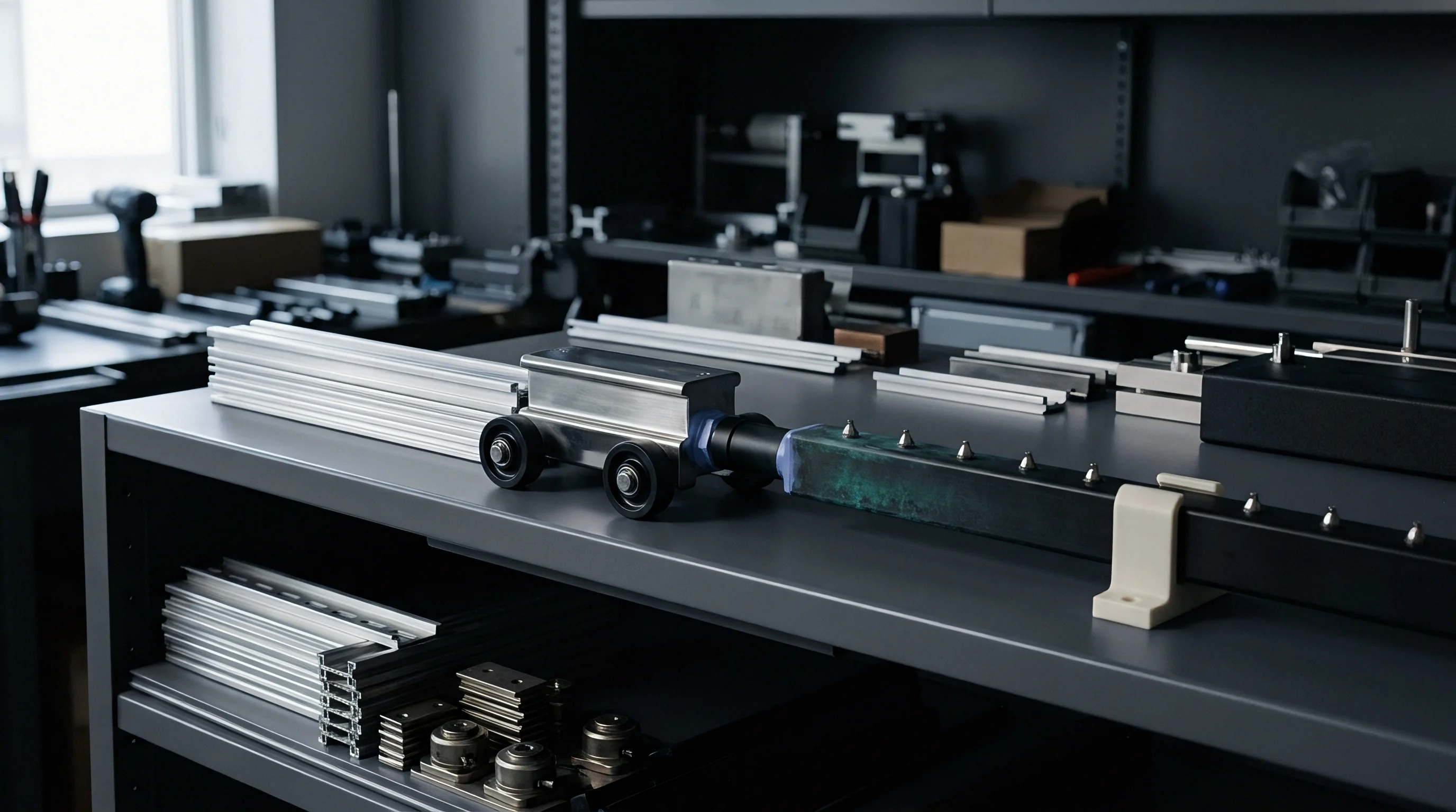
Mounting mechanics inside the thermal test apparatus dictate the boundary conditions of the mechanical stress field. Thermal expansion differences between the device under test, the carrier printed circuit board, and the structural test jig introduce extraneous stresses that register on the proof mass as apparent acceleration. High-grade verification requires an evaluation apparatus engineered with isotropic thermal behavior and high rigidity.

Mechanical Interface Mechanics
Direct solder attachment of quad-flat no-leads packages to thick, multi-layer FR4 material induces substantial package warpage over temperature. The glass transition temperature of standard FR4 sits between one hundred thirty and one hundred forty degrees Celsius, yet its coefficient of thermal expansion changes abruptly across the operating range, shifting from fourteen parts per million per Kelvin in the in-plane axes to over sixty parts per million per Kelvin in the out-of-plane axis. Ceramic printed circuit boards made from aluminum oxide provide a matched thermal expansion coefficient of approximately six to seven parts per million per Kelvin, aligning closely with the package molding compound.
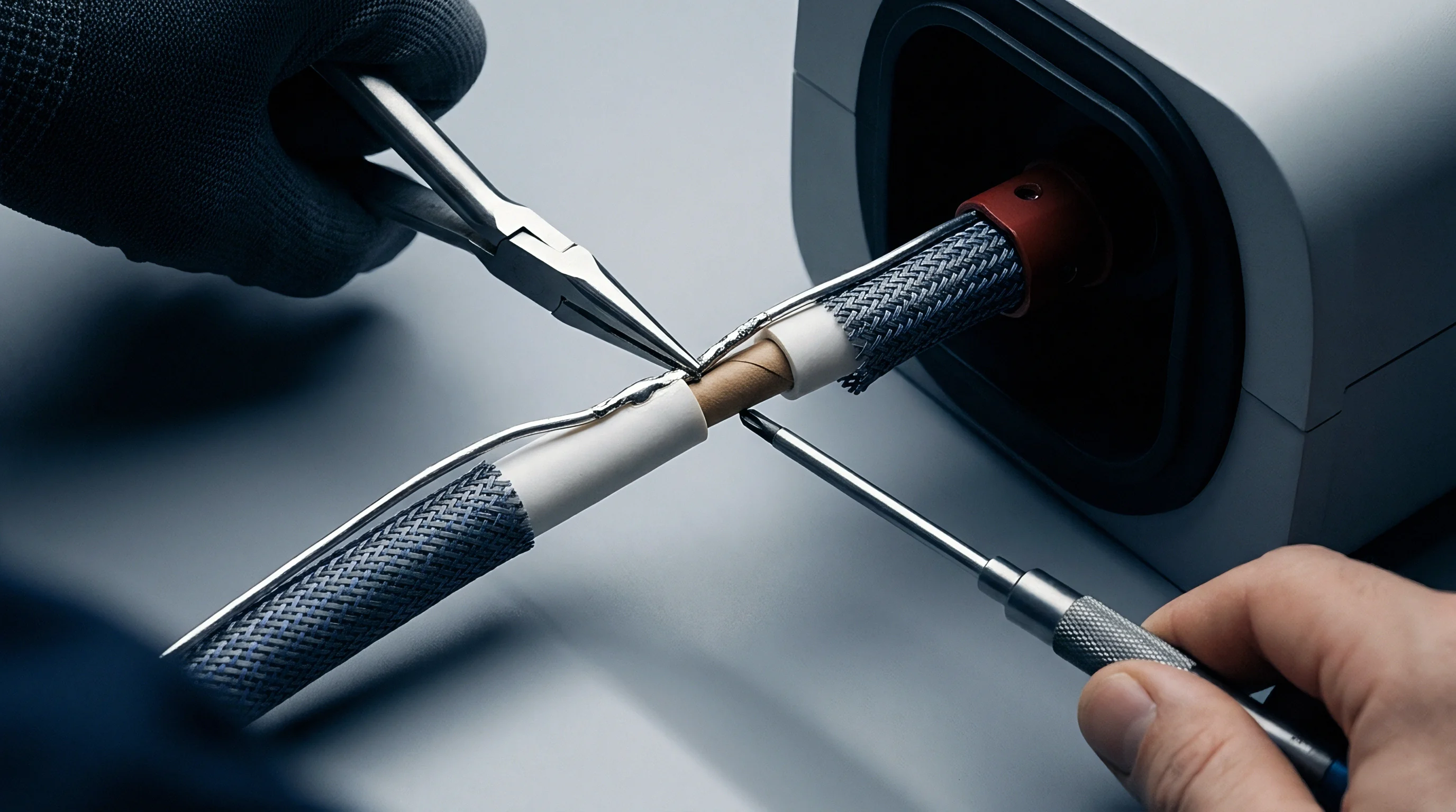
Cantilevered circuit boards induce parasitic bending moments under turbulent convection airflows within environmental chambers. Rigid clamp frames manufactured from low-expansion alloy materials hold the test assembly under controlled mechanical boundary conditions.
| Substrate Material | CTE In-Plane (ppm/K) | CTE Out-of-Plane (ppm/K) | Thermal Conductivity (W/m-K) | Young Modulus (GPa) |
|---|---|---|---|---|
| Standard FR4 Laminate | 14.2 | 65.0 | 0.35 | 22.0 |
| High-Tg FR4 Laminate | 12.5 | 48.0 | 0.40 | 24.5 |
| Alumina Ceramic (Al2O3) | 6.8 | 6.8 | 28.0 | 330.0 |
| Aluminum Nitride (AlN) | 4.5 | 4.5 | 170.0 | 310.0 |
| Silicon Carrier Plate | 2.6 | 2.6 | 149.0 | 160.0 |
Spring-loaded test sockets introduce uncontrolled, temperature-dependent contact resistance and variable clamping forces that compromise low-noise micro-volt readout operations. Solder evaluation boards down with low-temperature bismuth-tin alloys or compliant indium-bearing solders when mechanical decoupling is paramount. Direct lead soldering with controlled standoff height preserves device calibration stability.

Convection Shielding and Enclosures
Forced-air environmental chambers generate rapid heat exchange through turbulent boundary layers on device packaging. Direct wind vectors over the component plastic body produce local surface cooling that induces dynamic mechanical torque across the internal cavity. Test engineers encapsulate the populated test cards inside solid copper or aluminum thermal equalization enclosures.
- Equalization blocks constructed from oxygen-free electronic copper absorb rapid turbulent temperature oscillations and redistribute incoming heat entirely through conductive conduction.
- Thermal interface pads with low Shore A hardness prevent excessive mechanical compression forces against the delicate sensor package during fixture assembly torque-down.
- Hermetic chamber barriers prevent condensation moisture ingress from altering parasitic surface leakage currents across high-impedance analog sensor pins at sub-zero temperatures.
The vendor claims offset instability during thermal ramp profiles stems entirely from external circuit board warp rather than internal anchor asymmetry.

Soak
Thermal testing regimes balance throughput cycle time against thermodynamic settling requirements. Fast thermal ramping obscures intrinsic zero-g drift through temporal lag, yielding apparent hysteresis loops that disappear under quasi-static soak sequences. Characterization programs deploy stepped thermal plateaus separated by controlled transition rates.

Ramp Rate Dynamics
Chamber air reaches a setpoint minutes before internal silicon proof masses achieve thermal equilibrium. Accelerometer components housed in ceramic leadless chip carriers display thermal time constants between twelve and thirty seconds, while thick high-density plastic enclosures reach steady-state conditions only after sixty to ninety seconds. Ramping chamber air faster than one Kelvin per minute produces dynamic temperature differentials between internal die-mounted thermistors and micromachined capacitive beams.
A thermal chamber ramp rate exceeding two degrees Celsius per minute introduces false hysteresis loops through internal structural lag.
Characterizing pure static offset drift demands ramp velocities capped at 0.5 Kelvin per minute. Step-and-soak trajectories hold the target plateau for a minimum of twenty minutes per fifteen-Kelvin increment. Settling verification uses consecutive readouts to prove zero drift over five-minute windows.
| Package Configuration | Thermal Mass (g) | Time to 99% Soak (s) | Apparent TCO Error at 5 K/min (°C Offset) |
|---|---|---|---|
| LGA 2x2x0.9 mm Plastic | 0.015 | 45 | 0.85 |
| QFN 4x4x1.2 mm Plastic | 0.065 | 110 | 2.10 |
| LCC-20 9x9x2.5 mm Ceramic | 0.480 | 420 | 6.40 |
| Kovar Can Hermetic Module | 4.200 | 1250 | 14.80 |
Data recorded before temperature stabilization compromises yield calculations. Thermal stabilization requires strict procedural timing.
Settling criteria apply to every step. The chamber environment demands patience.
Hysteresis and Mechanical Settling
Plastic deformation of packaging compounds manifests as closed-loop offset hysteresis. Sweeping temperature from room ambient up to eighty-five degrees, down to minus forty, and back to ambient exposes non-reversible stress shifts within the die-attach resin. Polymeric cross-linking shifts, filler particle rearrangement, and moisture release during the bake phase introduce unrecoverable mechanical offsets.
A component exhibiting a linear offset drift of one milli-g per Kelvin during upward heating can show a two milli-g permanent shift upon returning to twenty-five degrees Celsius.
Thermal preconditioning cycles clear production processing stresses prior to baseline calibration data acquisition. Test engineers subject uncalibrated lots to three unpowered deep thermal cycles across the full operating range. This stress release sequence stabilizes the polymer chain structure before logging data for register coefficient generation.
True thermal equilibrium reveals itself when reversal curves collapse onto a single trace.

Extraction
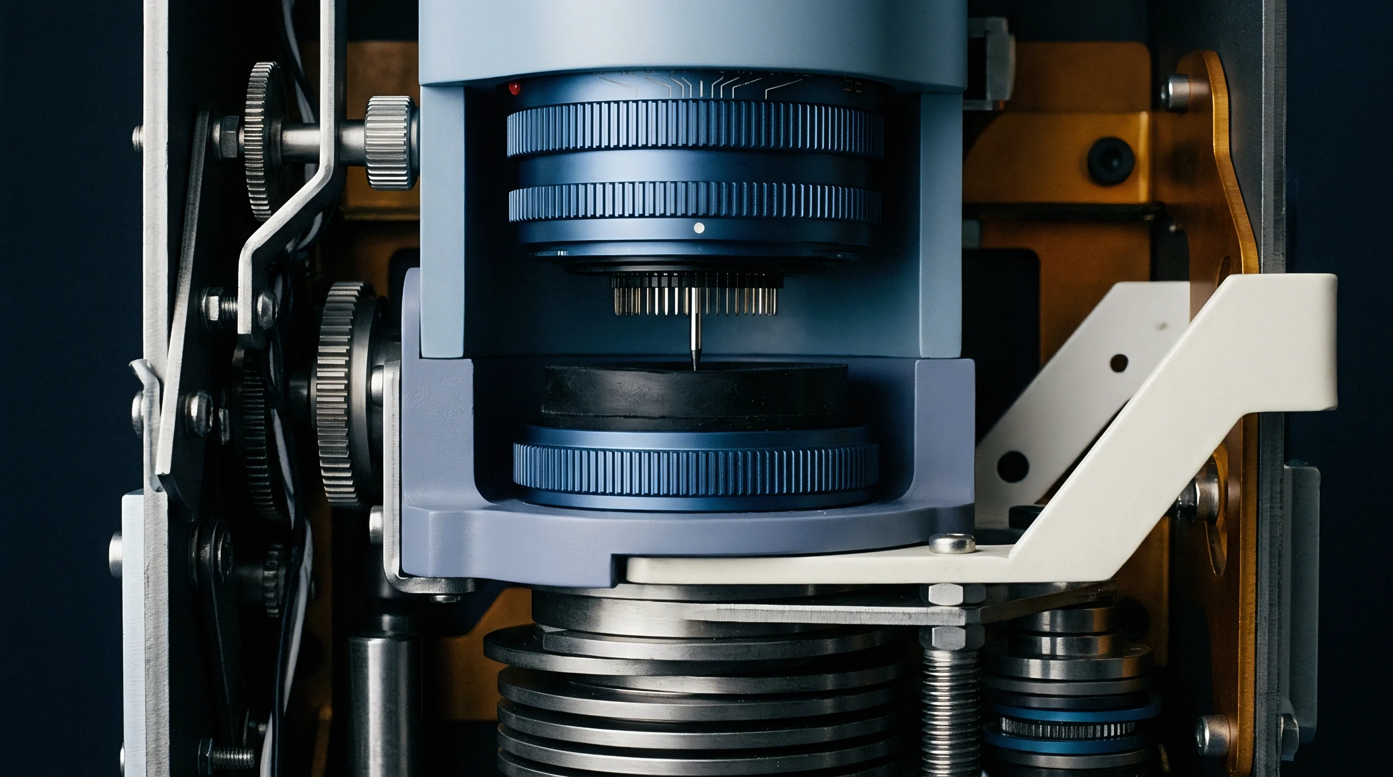
Separating gravitational vectors from intrinsic electrostatic and mechanical offsets requires controlled spatial orientation during the thermal cycle. Gravity acts as an omnipresent acceleration field of one g. If the device shifts or the test fixture tilts by a fraction of a milliradian during thermal expansion of the test bench, the gravitational projection onto the sensitive axis alters the measurement record.

Multi-Position Inversion Protocols
Tumble testing isolates zero-g bias from scale factor variations. An accelerometer mounted to a precision multi-axis indexing head experiences positive one g and negative one g static gravitational loads when flipped one hundred eighty degrees relative to true vertical.
Subtracting the negative one g reading from the positive one g reading eliminates the zero-point offset entirely, leaving pure sensitivity. Adding the two readings together cancels the acceleration vector completely, isolating twice the true zero-g offset:
V_offset(T) = / 2
S(T) = /
Executing this two-position inversion at every thermal plateau separates the Temperature Coefficient of Offset from the Temperature Coefficient of Sensitivity. Performing the full profile across orthogonal orientations extracts cross-axis sensitivity drift simultaneously.
A fixture tilt drift of fifty microradians over temperature simulates fifty micro-g of uncalibrated accelerometer offset shift.
Dividing the mathematical calculations across multiple axes exposes cross-axis coupling. Structural testing demands rigorous verification of all rotational angles.
Mathematical Parameter Modeling
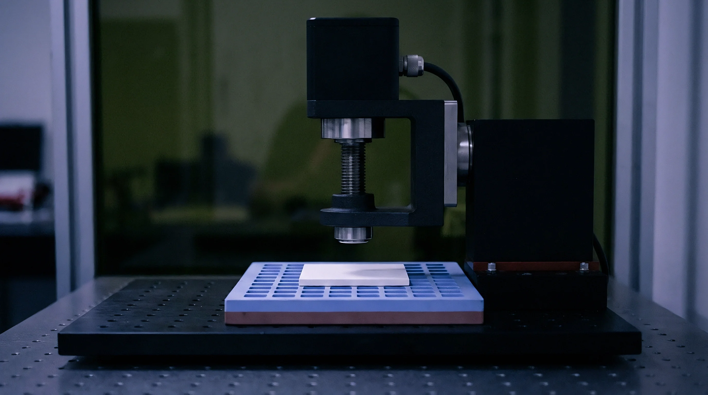
Raw offset data plotted across temperature requires mathematical curve fitting for register-based digital compensation algorithms. Third-order polynomial models capture both inflection points and asymptotic mechanical behaviors observed near temperature extremes.
B-spline interpolation handles localized non-linearities caused by package resonance changes, whereas second-order Chebyshev polynomials minimize truncation ripple across closed industrial envelopes. Residual errors after polynomial extraction define the uncompensated offset stability.
- Raw offset acquisition collects baseline zero-bias registers across all target temperature plates at established thermodynamic equilibrium.
- Least-squares polynomial regression computes second-order and third-order compensation coefficients mapped to internal silicon temperature sensor registers.
- Cross-axis projection screening removes residual mechanical tilt errors introduced by thermal warpage of the indexing fixture shafts.
- Residual verification sweeps validate that post-compensation bias drift remains within customer specification bounds across all operational operational sectors.
A persistent unresolved dilemma concerns whether residual high-order drift components stem from physical silicon anchor deformation or micro-volt reference drift inside the application-specific integrated circuit bandgap.

Yield
Calibration time within multi-position environmental chambers drives testing costs for precision inertial sensors. Consumer devices with loose performance bands bypass continuous temperature testing through wafer-level static trimming or room-temperature offset screening. Industrial, aerospace, and high-performance navigation sensors demand comprehensive multi-temperature qualification, where long chamber dwell times scale testing costs exponentially.

Commercial Binning and Calibration Economics
A multi-position temperature calibration run spanning negative forty to positive eighty-five degrees Celsius requires approximately four hours of automated chamber time per panel. With chamber operating costs and capital depreciation on rate-table test equipment totaling seventy-five dollars per hour, a test cycle costs three hundred dollars per batch. Distributing that burden over a tray of one hundred parts adds three dollars per unit in direct test expense.
Silicon foundries and automated test equipment houses use algorithmic batch modeling to reduce testing duration. Single-point offset trims performed at twenty-five degrees Celsius correct for mechanical release tolerances, leaving raw thermal drift uncorrected. Premium parts undergo two-point calibration at room ambient and elevated temperature, cutting processing time to forty minutes while screening out outliers with extreme second-order curvature.
| Screening Strategy | Test Duration (Minutes) | Direct Test Cost per Unit (USD) | Typical TCO (mg/K) | Yield Fall-Off (%) |
|---|---|---|---|---|
| Single Ambient Trim (25°C) | 0.08 | 0.02 | 0.150 | 1.2 |
| Two-Point Factory Calibration | 35.00 | 0.65 | 0.040 | 4.8 |
| Three-Point Stepped Profiling | 110.00 | 1.85 | 0.015 | 11.5 |
| Full Multi-Position Chamber Profile | 240.00 | 3.10 | 0.002 | 18.2 |
Rejection rates increase significantly as offset drift requirements tighten below 0.05 milli-g per Kelvin. Wafers with uneven deep reactive-ion etching profiles show wide radial distributions of thermal coefficients, causing yield fallout at the wafer perimeter during full-temperature verification.
Contractual Specification Lines
Procurement documents must delineate the exact physical conditions governing offset drift limits. Ambiguous definitions allow vendors to quote best-fit linear drift slopes measured on bare silicon dies rather than packaged assemblies mounted to circuit boards. Standard purchase contracts mandate explicit performance clauses.
The standard procurement agreement must specify compliance with IEC 60747-14-1 or IEEE 1293-1998, requiring offset drift to remain within stated numerical limits across continuous temperature cycling at specified ramp rates without device re-zeroing, which eliminates supplier reliance on idealized factory room-temperature trims.