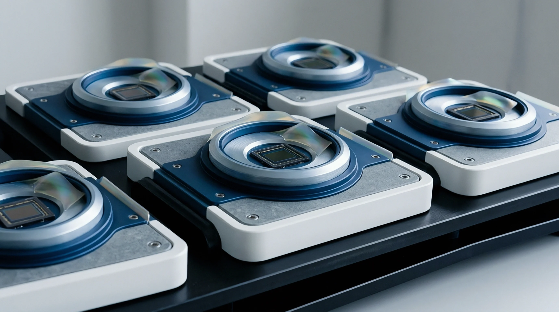
Measurement Mechanism
A piezoresistive stress sensor functions as a transducer that converts mechanical strain into an electrical resistance variation through the modification of the band structure in a semiconductor crystal. The piezoresistive stress sensor relies on the change in carrier mobility and concentration when an external force deforms the lattice. High precision requires thermal compensation because temperature fluctuations alter the base resistance independent of the applied load.
Sensitivity Characterization
Gauge factor values define the performance of a piezoresistive stress sensor by relating the fractional change in electrical resistance to the mechanical strain. Manufacturers quantify this ratio against a known reference strain applied through a cantilever beam or a four point bending fixture. Nonlinearity emerges when the deformation exceeds the linear elastic limit of the substrate, causing permanent lattice displacement or material fatigue.
Calibration curves provide the correction coefficients required to linearize the output voltage across the intended operating range of the device.
Installation Interface
Mounting techniques for a piezoresistive stress sensor dictate the accuracy of the mechanical coupling between the transducer and the host surface. Adhesive bonding layers transfer force to the sensor body without introducing excessive creep or signal attenuation. Thermal expansion mismatches between the sensor package and the mounting surface introduce parasitic stresses that skew the measurement data.
Rigid housing designs minimize these effects by shielding the sensing element from thermal gradients or ambient airflow.
Signal Processing
Integrated circuits amplify the low level differential signals produced by a piezoresistive stress sensor to bridge the gap between microscopic resistance changes and readable data formats. Bridge configurations such as the Wheatstone circuit reject common mode interference to produce a stable voltage proportional to the measured strain. Digital sampling hardware must accommodate the bridge excitation frequency to prevent aliasing during high speed data acquisition.
Resolution limits derive from the noise floor of the electronic amplifier rather than the mechanical sensitivity of the crystal structure itself.