
Precision Bandgap Thermal Stress Error Reduction across Surface Mount Packages
Mitigate bandgap thermal stress errors using compliant leaded packages, PCB isolation slots, polyimide die buffers, and stabilized factory calibration.
Mitigate bandgap thermal stress errors using compliant leaded packages, PCB isolation slots, polyimide die buffers, and stabilized factory calibration.

Optimized PCB slotting isolates precision voltage references from board strain and thermal gradients, cutting drift below one part per million.

Asymmetric thermal expansion shifts bandgap voltage via piezoresistive substrate stress; mechanical slots and ceramic packaging isolate critical reference nodes.

Board flexure stress couples to analog dies via solder joints and mold compounds, shifting bandgap voltages up to 10 millivolts under thermal cycling.

Monolithic reference thermal drift sensitivity combines silicon junction non-linearities, piezoresistive mechanical package stress, and solder reflow hysteresis.

MEMS thermal hysteresis creates non-repeatable zero-g offset shifts up to 3 mg, driving uncompensable arcsecond tilt errors in static leveling systems.
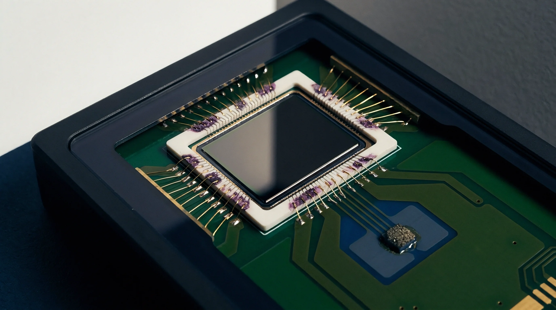
WLCSP packages transfer board thermal strain directly to the die, causing reference drift, while ceramic cavity housings eliminate mechanical coupling.
Expertise is a utility, not a secret. sentiention™ publishes its working knowledge as open reference: intelligence layer covering the materials it sources, the markets it enters, and the reference that serves both.