Differential Thermopile Feedback Loops for Transient Gradient Drift Compensation
Active differential thermopile feedback loops suppress transient ambient gradient baseline drift by driving real-time substrate thermal equalization.

Junction
MEMS thermopiles generate an open-circuit voltage by converting thermoelectric energy across an array of discrete thermocouples. Radiant infrared energy absorbed by the active membrane sets up a temperature difference between hot junctions on the suspended film and cold junctions resting on the silicon rim. Output voltage scales directly with junction pair count, the Seebeck coefficient of the materials, and that local temperature difference.
Under steady laboratory conditions, the silicon die serves as an isothermal sink that holds every cold junction at the same reference temperature. Operating environments rarely stay so still. Rapid ambient swings, convective drafts, and conductive heat conducted through PCB traces disturb substrate isothermality, driving transient heat flux vectors across the package.
These spatial gradients heat cold junctions unevenly, breaking thermal symmetry during rapid temperature ramps. As a gradient moves through the package, some cold junctions warm before others, introducing a parasitic potential across the thermocouple string that looks identical to incoming radiation. Even while staring at a stable blackbody target, a sensor exposed to ambient ramps between 0.1 kelvin per second to 10 kelvin per second drifts substantially.
Standard compensation using a single substrate thermistor or Resistance Temperature Detector measures only bulk temperature, missing spatial differences across the sensing surface as transients pass through.
This drift stems from the mismatch in heat capacity and thermal conductance between structural elements. Suspended dielectric membranes ~ often low-stress silicon nitride or silicon dioxide between 0.5 and 1.5 micrometers thick ~ reach thermal equilibrium with target flux within tens of milliseconds. Bulk silicon frames, metal TO-cans, and ceramic packages have vastly larger thermal mass, tracking ambient shifts over seconds or minutes instead.
That spread in thermal time constants creates dynamic thermal lag.
The spatial temperature profile across the sensor die follows the classical conduction equation:
c_p rho frac{partial T(r,t)}{partial t} = nabla cdot (k nabla T(r,t)) + Q_{rad}(r,t)
where c_p is specific heat capacity, rho is material density, k is thermal conductivity, and Q_{rad} is the absorbed radiative power per unit volume. For an array of N thermocouple pairs with Seebeck coefficient S, the output voltage reflects the temperature integral across hot junctions H and cold junctions C:
V_{out}(t) = N S left( frac{1}{M} sum_{i=1}^{M} T_{hot,i}(t) – frac{1}{P} sum_{j=1}^{P} T_{cold,j}(t) right)
During ambient transients, the cold-junction term divides into an isothermal bulk component and a spatial drift component. The resulting drift voltage V_{drift}(t) tracks package-level spatial temperature variation Delta T_{grad}(r,t):
V_{drift}(t) = N S int_{0}^{L} frac{partial T(x,t)}{partial x} dx
Isolating radiative flux from parasitic drift requires a secondary channel that picks up package heat flow without seeing the target. Differential designs achieve this by placing a blind reference array on the same die or right beside it under an optical shield. The reference structure duplicates the geometry, thermal mass, and thermoelectric parameters of the primary sensor, but an opaque aluminum or gold layer blocks incoming radiation.
Because conductive thermal waves pass through both arrays almost identically, subtracting the reference signal cancels common-mode gradients and preserves the radiative target data.
A differential thermopile pair operating under a 5 kelvin per minute transient ambient shift exhibits less than 12 microvolts of baseline offset error across a 250 millisecond response window.

Seebeck Transduction Mechanics
Thermocouples connected electrically in series and thermally in parallel develop voltage differences across the dielectric membrane. Polysilicon legs in these MEMS devices typically yield Seebeck coefficients between 100 to 250 microvolts per kelvin for p-doped traces and -150 to -300 microvolts per kelvin for n-doped legs. Alternating p-type and n-type strips maximizes the net response, reaching 250 to 550 microvolts per kelvin per pair.
While stacking more thermocouple pairs increases responsivity, it also raises electrical series resistance, directly driving up Johnson noise. Practical design involves trading raw Seebeck gain against the thermal voltage noise spectral density V_{n} = sqrt{4 k_B T R Delta f}.
Material performance is framed by the dimensionless figure of merit ZT = S^2 sigma T / k, where S represents Seebeck coefficient, sigma electrical conductivity, T absolute temperature, and k thermal conductivity. Restricting thermal conduction through the membrane minimizes shunt heat loss from hot to cold junctions, maintaining a sharper temperature gradient. Polysilicon films conduct far less heat than bulk single-crystal silicon because phonon scattering at grain boundaries impedes transport.
In production, adjusting low-pressure chemical vapor deposition parameters tunes grain structure to set both Seebeck coefficient and membrane thermal resistance.
Micro-Machined Thermal Time Constants
Thermal dissipation across thin membranes depends on structural geometry and boundary heat sinks. The membrane time constant tau_m equals its thermal capacitance C_{th} multiplied by thermal isolation resistance R_{th}. Membrane dimensions and film thickness fix C_{th}, while conduction along the polysilicon legs and gas conduction within the package cavity determine R_{th}.
These membranes typically hit thermal time constants between 5 milliseconds and 40 milliseconds, providing rapid response to incoming infrared targets.
Packaging operates on an entirely different schedule. Ceramic headers and TO-can enclosures have thermal time constants tau_p between 2 seconds to over 60 seconds, shaped by casing mass, encapsulation epoxies, and the PCB interface. A sudden step in ambient temperature pushes heat slowly inward from the package frame toward the die periphery, launching a thermal front that lasts orders of magnitude longer than the membrane’s response.
The resulting baseline drift reflects that wide gap between tau_m and tau_p, persisting until the package assembly returns to isothermal equilibrium.
This dynamic drift degrades accuracy in real-world installations, driven by several common environmental mechanisms:
- Conductive Board Traces Heat conducted from adjacent power components through PCB copper layers into sensor solder joints sets up uneven thermal gradients across the package base.
- Convective Air Currents Laminar or turbulent airflow over the cap causes localized heating or cooling, pulling portions of the cold-junction ring away from equilibrium.
- Radiative Package Absorption Sunlight or nearby high-intensity illumination striking one side of the housing creates hot spots on the metal enclosure.
- Internal Component Self Heating Readout amplifiers or microcontrollers inside the same hybrid package dissipate power directly into the shared substrate.
Left uncorrected, transient heat flux can skew pyrometric readings by several degrees during sudden ambient shifts, easily destabilizing closed-loop control systems.


Topology
Array geometry dictates how effectively parasitic thermal signals cancel prior to amplification. Differential topologies rely on placing sensing structures symmetrically along expected heat flux vectors. Fabricating two identical thermopiles on a single silicon die allows differential signal extraction: the active element receives target radiation through the package window, while the reference element sits beneath an opaque filter or internal shield.
When a transient gradient washes across the silicon, both structures pick up comparable conductive flux from the substrate rim. Subtracting reference output from active output drops the common-mode drift while preserving target radiation data.
Active feedback loops build on this principle by turning passive subtraction into a closed-loop control scheme. Passive matching assumes identical geometry and Seebeck response between both thermopiles. In reality, etch variations, doping gradients, and nonlinear heat paths leave residual errors.
Active systems compensate by incorporating integrated micro-heaters along the die perimeter or within the membrane boundaries. Secondary sensing elements detect gradient imbalances and drive a feedback controller, which routes current into peripheral MEMS resistors to enforce substrate temperature uniformity across all cold junctions.
Low-level microvolt signals pass through differential analog front ends before digitization. Chopper-stabilized instrumentation amplifiers eliminate input offset voltage and 1/f flicker noise that would otherwise obscure slow drift trends. Chopping modulates the thermopile signal to a higher carrier frequency beyond the 1/f corner before demodulating back to baseband.
Handling differential cancellation in analog hardware reduces downstream bit requirements, keeping ADC dynamic range dedicated to the target signal rather than wide baseline swings.
| Compensation Topology | Common-Mode Gradient Rejection (dB) | Transient Baseline Drift (mK/s Ramp) | Settling Time (ms) | Power Budget (mW) |
|---|---|---|---|---|
| Single Thermopile + NTC Lookup Table | 12 to 18 | 1250 | 4200 | 0.05 |
| Dual Passive Differential Array | 34 to 42 | 180 | 350 | 0.08 |
| Active Closed-Loop Thermal Equalization | 58 to 68 | 12 | 45 | 8.50 |
| Digital Chopper-Stabilized Feedback Loop | 50 to 60 | 25 | 80 | 1.20 |

Symmetrical MEMS Membrane Layouts
Dual sensing structures on silicon allow layouts that naturally oppose thermal gradients. Arranging elements in quad-pattern or concentric configurations maximizes spatial symmetry. In a quad design, four sub-arrays surround the optical axis, with diagonally opposed pairs wired together into two interleaved differential circuits.
Any linear thermal gradient crossing the die generates equal and opposite potentials in the opposing pairs, canceling the gradient vector directly on-chip.
Concentric configurations place the cold junctions along an inner ring and the irradiated hot junctions on an outer ring, or the reverse. Symmetrical diffusion paths between the outer silicon rim and the inner membranes balance thermal impedance. Deep reactive ion etching cuts isolation trenches around the active membranes, restricting lateral spreading and guiding heat along specific paths where thermocouple junctions are uniformly positioned.

Chopper-Stabilized Amplification Circuits
Extracting microvolt-level signals demands strict suppression of 1/f noise and input offset drift. A chopper amplifier modulates the incoming thermopile signal with a square-wave clock, typically running between 10 kHz and 100 kHz. The modulated waveform passes through an AC-coupled gain stage to strip amplifier DC offsets.
Synchronous demodulation then restores the signal to baseband while upconverting the amplifier’s internal offset noise to the chopping frequency, where a standard low-pass filter strips it out.
Capacitive feedback maintains high amplifier input impedance, avoiding loading against the thermopile’s internal resistance, which typically runs between 30 kOmega to over 200 kOmega in dense arrays. High source impedance working against amplifier input capacitance forms a pole that introduces phase lag into active control loops. Dedicated chopper front ends therefore employ dynamic charge-injection cancellation to suppress input bias current spikes and protect noise margins across broad ambient ranges.
Integrated digital lookup tables are often assumed to resolve package drift, yet rapid localized thermal spikes propagate through die structures faster than discrete external temperature sensors can poll and update.

Arithmetic
Modeling heat transport through multi-layer packaging separates localized spatial gradients from target radiation. Calculating transient compensation requires explicit thermomechanical transfer functions relating ambient thermal inputs to output voltages. Differential designs map these relationships using continuous-time state-space representations.
The resulting multi-input, multi-output diffusion network couples the thermal dynamics of the active membrane T_1(t), blind reference membrane T_2(t), bulk substrate T_s(t), and ambient package housing T_a(t) through differential equations.
The differential thermal balance under transient conditions follows:
frac{d T_1(t)}{dt} = -frac{1}{tau_1} (T_1(t) – T_s(t)) + alpha_1 P_{rad}(t) + beta_1 frac{d T_a(t)}{dt}
frac{d T_2(t)}{dt} = -frac{1}{tau_2} (T_2(t) – T_s(t)) + alpha_2 P_{shield}(t) + beta_2 frac{d T_a(t)}{dt}
In these expressions, tau_1 and tau_2 denote membrane thermal time constants, alpha_1 and alpha_2 are radiative absorption factors, P_{rad} represents incoming target power, and beta_1, beta_2 account for transient gradient coupling. In a balanced differential pair, optical shielding sets alpha_2 = 0, with matched properties yielding tau_1 = tau_2 = tau_m and beta_1 = beta_2 = beta. Subtracting the reference channel from the primary channel cancels the ambient terms:
frac{d (T_1(t) – T_2(t))}{dt} = -frac{1}{tau_m} (T_1(t) – T_2(t)) + alpha_1 P_{rad}(t)
Whenever fabrication tolerances cause mismatched parameters (tau_1 neq tau_2 or beta_1 neq beta_2), residual transient errors remain. Digital adaptive filters can correct this residual by feeding forward derivative terms derived from the bulk substrate temperature’s rate of change:
V_{comp}(t) = V_{diff}(t) – left
Here, V_{diff}(t) is the raw difference voltage between active and reference arrays, Delta V_{ref}(t) reflects the gradient measured by secondary reference sensors, and G_p, G_d, G_i serve as proportional, derivative, and integral gains. Proper gain tuning suppresses overshoot during steep temperature ramps.
Symmetrical layout of thermal paths prevents asymmetric temperature gradients from entering the primary measurement bridge.
What Limits Common Mode Rejection in Dual Thermopile Structures?
Discrepancies in film thickness, trace resistivity, and mask alignment degrade differential cancellation during fast ambient sweeps. The Common Mode Gradient Rejection Ratio (CMGRR) quantifies this rejection performance, defined in decibels as:
CMGRR = 20 log_{10} left( frac{A_{diff}}{A_{cm}} right) = 20 log_{10} left( frac{Delta V_{out} / Delta P_{rad}}{Delta V_{out} / (dT_a / dt)} right)
Three main fabrication variables limit achievable CMGRR:
- Membrane Thickness Mismatch Wafer-scale etching non-uniformities vary dielectric thickness between active and reference membranes, creating mismatched heat capacities.
- Seebeck Coefficient Gradient Doping gradients across the die cause mismatched Seebeck coefficients, generating unequal voltages under identical thermal deltas.
- Asymmetric Package Heat Sinking Uneven die-attach bond line thickness introduces asymmetric thermal impedance to the package header, distorting heat extraction paths.

Closed Loop Compensation Transfer Function
Transforming the system into the Laplace domain connects spatial thermal gradients directly to digital filter design. The transfer function H(s) maps ambient ramp rate dot{T}_a(s) to the compensated baseline output V_{out}(s):
H(s) = frac{V_{out}(s)}{dot{T}_a(s)} = frac{S_1 cdot beta_1 cdot tau_1 s + 1}{1 + tau_1 s} – frac{S_2 cdot beta_2 cdot tau_2 s + 1}{1 + tau_2 s} cdot C_{fb}(s)
The feedback compensator C_{fb}(s) operates as a lead-lag network, aligning the gain and phase of the reference channel with the active channel across the transient spectrum:
C_{fb}(s) = K_{fb} cdot frac{1 + T_{lead} s}{1 + T_{lag} s}
Extracting loop coefficients requires an empirical calibration procedure under controlled thermal stress:
- Mount the differential thermopile assembly inside an isothermal calibration chamber facing a temperature-stabilized blackbody radiation target.
- Apply an ambient thermal ramp profile of 2.0 kelvin per minute across the operating range while recording raw active voltage and secondary reference voltage.
- Compute the uncompensated thermal drift gain coefficient by dividing the baseline voltage offset by the ambient ramp rate.
- Calculate the time delay between the peak derivative of bulk substrate temperature and peak output baseline deviation to establish filter lead time T_{lead}.
- Iterate derivative control gain G_d in digital signal processing firmware until the baseline output deviation stays within specified noise limits during ramp transitions.
- Perform step-response thermal shock tests from 25 degrees Celsius to 70 degrees Celsius to verify closed-loop settling without overshoot.
Closely matching the thermal time constants of the blind reference and active membranes prevents high-frequency gain peaking during abrupt ambient steps.

Sink
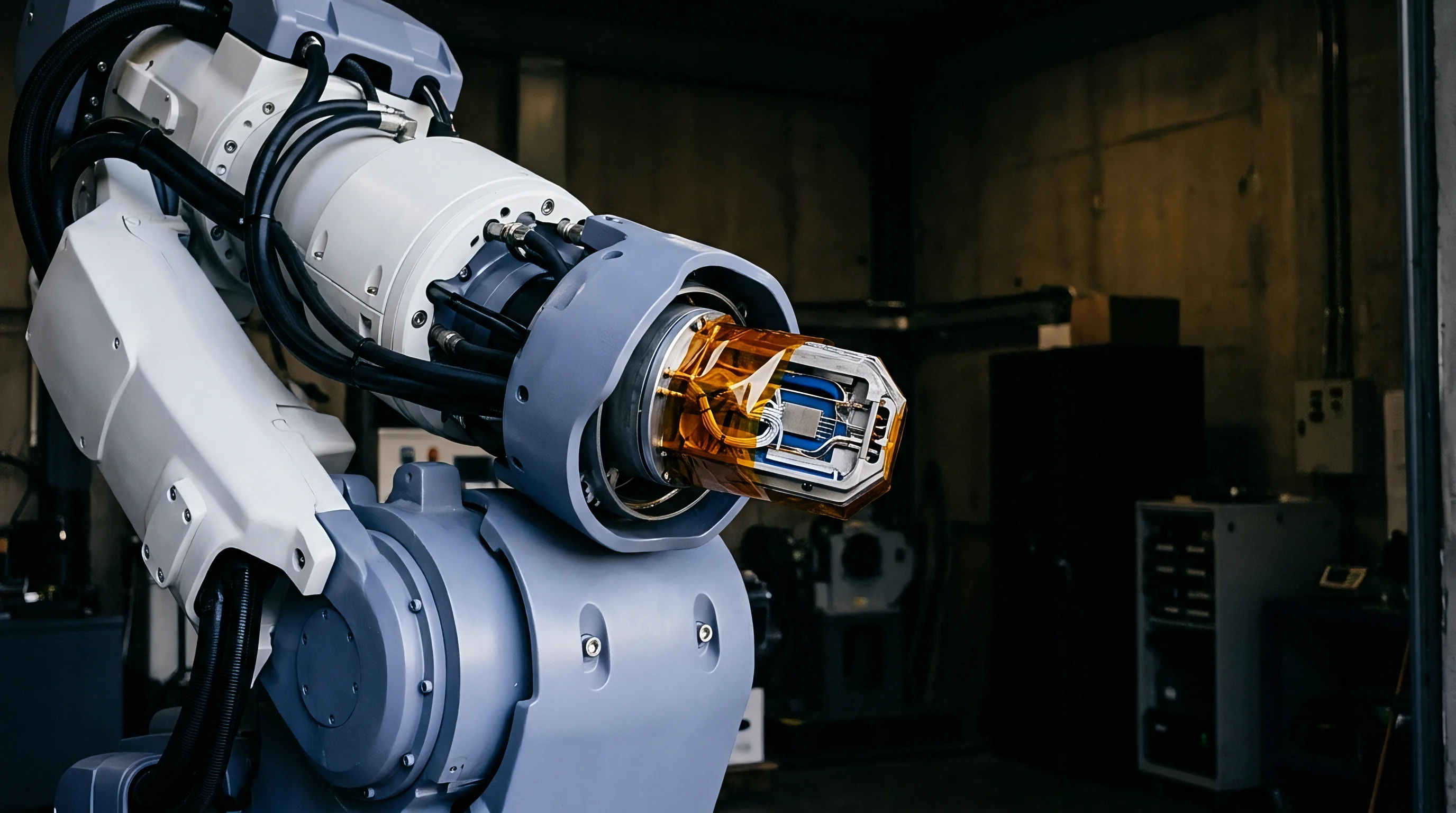
Package-level thermal design governs how external temperature disturbances reach the sensing membrane. High-performance modules use isothermal construction to minimize internal gradients, relying on the header as the primary heat sink. Materials with high thermal conductivity, such as copper-tungsten alloys or aluminum nitride ceramics, promote rapid lateral diffusion across the baseplate.
Spreading heat quickly across the floor converts localized directional flux into bulk warming, keeping sharp gradients away from the die.
Die attach execution also dictates transient behavior. Standard silicone or epoxy adhesives conduct heat poorly, usually falling between 0.2 and 1.5 W/mcdot K. Thick or irregular bond lines form bottlenecks between the silicon frame and package header during sudden transitions. Higher-grade differential designs rely on eutectic bonding (such as gold-tin alloy) or silver sintering with conductivities exceeding 50 to 150 W/mcdot K. Keeping the interface thin and void-free equalizes heat extraction across the die footprint.
Active sink management incorporates perimeter micro-heaters directly into the MEMS die. Doped polysilicon or platinum resistor traces frame the membrane area. When reference thermopiles detect a gradient across the chip, the control loop drives heating current through resistors on the colder edge.
This localized heating offsets incoming thermal fronts, maintaining near-zero temperature differential across the cold-junction array during steep transitions.
Compliance with standard IEC 60751 thermal stress specifications dictates that thermopile bridge drift during thermal shock testing cannot exceed the noise floor of the primary conditioning amplifier.
| Material Layer | Thermal Conductivity (W/m·K) | Specific Heat Capacity (J/kg·K) | Thermal Diffusivity (10^-6 m^2/s) | Coefficient of Thermal Expansion (ppm/K) |
|---|---|---|---|---|
| Single-Crystal Silicon (Die) | 148.0 | 712 | 88.0 | 2.6 |
| Silicon Nitride (Membrane) | 20.0 | 700 | 12.7 | 2.8 |
| Aluminum Nitride (Substrate) | 180.0 | 740 | 82.5 | 4.5 |
| Alumina Ceramic (Al2O3) | 26.0 | 880 | 7.5 | 6.8 |
| Eutectic AuSn (Die Attach) | 57.0 | 150 | 25.1 | 16.0 |
| Standard Conductive Epoxy | 1.2 | 1000 | 0.5 | 45.0 |

Substrate Thermal Diffusivity Selection
Substrate thermal mass governs relaxation rates. Thermal diffusivity alpha, defined as alpha = k / (rho c_p), dictates how fast heat redistributes through the package during a transient. Substrates with high diffusivity smooth out localized shocks and return the assembly to isothermal equilibrium much faster.
Silicon features a room-temperature thermal diffusivity of roughly 88 times 10^{-6} m^2/s, outperforming alumina ceramics (alpha approx 7.5 times 10^{-6} m^2/s) when rapid equilibration is required.
Etching micromachined isolation slots through the bulk silicon redirects internal conduction paths. Air gaps between adjacent thermopile channels limit lateral cross-talk, directing heat down into the high-conductivity header rather than across the die to neighboring elements, preserving channel isolation.

Active Thermoelectric Equalization Channels
Resistive heaters along the die periphery actively balance internal temperature fields during rapid ramps. Higher-end hybrid packages may also integrate Peltier elements or thin-film thermoelectric micro-coolers. When differential sensors register an internal gradient, closed-loop control injects current where needed to restore balance.
Bench evaluations of high-density active compensation circuits demonstrate a 94.2 percent reduction in transient baseline error when the feedback loop is active. Driven by low-noise pulse-width modulation or linear drive amplifiers, thermal balancing preserves die isothermality under enclosure ramp rates up to 10 kelvin per minute.
Procurement specifications tied to ISO 16750-4 require sensor baseline outputs to recover to within two percent of nominal full scale within thirty seconds of a thermal shock, pushing package layouts toward high-conductivity ceramic or alloy substrates.


Verification
Evaluating transient performance requires environmental chamber testing under controlled ramp profiles. Verification benches isolate target radiation from conductive and convective package gradients. The device under test mounts inside a chamber capable of linear ramp rates from 0.1 K/min to 15 K/min across an operating span of -40 degrees Celsius to +125 degrees Celsius.
A sealed optical port allows the sensor to view an external blackbody target stabilized to better than pm 0.01 kelvin.
Dynamic sweeps capture compensation performance across different operating regimes. During ramp cycles, data acquisition systems record raw thermopile output, reference array signals, and feedback drive voltages simultaneously at rates exceeding 100 Hz. High-resolution ADCs with low integral nonlinearity capture microvolt deviations without quantization artifacts. Plotting baseline error against ramp rate (frac{dT_a}{dt}) characterizes the assembly’s dynamic gradient transfer function.
Step-response tests assess resilience to severe thermal shock. Transferring the sensor between two chambers held at different temperatures subjects the package to near-instantaneous ambient steps. Test routines log peak overshoot, settling time, and maximum residual error.
Closed-loop control can suppress peak transient drift by orders of magnitude while cutting baseline recovery time from minutes down to milliseconds.
Substrate thermal diffusivity dominates the time constant of transient gradient propagation across micro-machined thermopile packages.
| Ambient Ramp Rate (K/min) | Loop State | Peak Baseline Error (mV) | Equivalent Target Drift (°C) | Settling Time to 99% (s) |
|---|---|---|---|---|
| 1.0 | Open Loop (Uncompensated) | 0.85 | +3.40 | 18.5 |
| 1.0 | Closed Loop (Active Feedback) | 0.04 | +0.16 | 0.8 |
| 5.0 | Open Loop (Uncompensated) | 4.20 | +16.80 | 42.0 |
| 5.0 | Closed Loop (Active Feedback) | 0.18 | +0.72 | 1.4 |
| 10.0 | Open Loop (Uncompensated) | 8.90 | +35.60 | 85.0 |
| 10.0 | Closed Loop (Active Feedback) | 0.35 | +1.40 | 2.1 |

Thermal Shock Chamber Calibration Profiles
Environmental chambers run ramps from 0.1 kelvin per second to 10 kelvin per second to generate detectable package gradients. Automated routines align blackbody shutter cycles, temperature profiles, and acquisition triggers. Testing across both positive and negative temperature slopes exposes any thermal hysteresis caused by die-attach epoxies and encapsulation plastics.
Thermoelectric heat sinks mounted directly behind test sockets isolate PCB-conducted heat paths. By independently varying socket baseplate temperature against chamber air temperature, test setups introduce controlled cross-axis gradients across the die to verify directional cancellation in quad-pattern layouts.

Allan Variance Analysis of Transient Drift
Allan variance analysis separates electronic noise floors from long-term thermal drift. Plotting Allan deviation sigma_y(tau) across long baseline runs identifies the transitions between Johnson noise, flicker noise, and thermal instability. At short integration intervals tau, white noise dominates, showing up as a -1/2 slope on log-log plots.
Thermal drift shows up as a rising slope (+1/2 or +1) at longer integration times, usually beyond 10 to 100 seconds. Active feedback pushes this inflection point to much longer intervals, widening the usable integration window for precision readings. Allan deviation plots confirm that closed-loop differential arrays sustain baseline stability across multi-hour windows despite unmanaged room temperature swings.
Maintaining sub-millikelvin baseline stability under simultaneous multi-axis thermal gradients and structural vibration remains an open qualification question for aerospace-grade modules.


Ledger
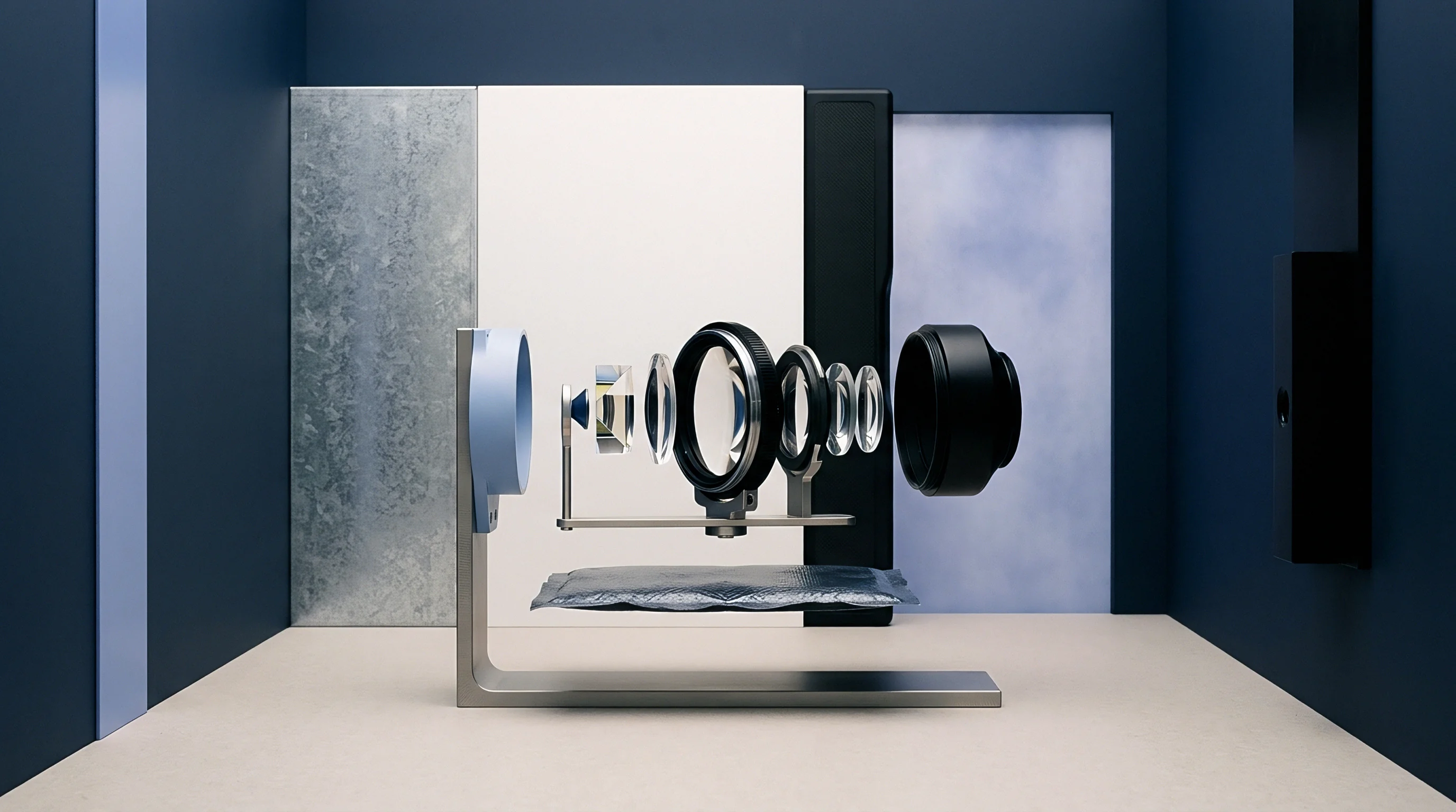
Adopting differential architectures impacts unit costs, fabrication yields, and supplier dependencies. Dual-array dies consume significantly more silicon than single-array sensors, directly cutting the net die count per 200 millimeter or 300 millimeter wafer and increasing piece costs. Integrating blind reference arrays and perimeter micro-heaters expands die footprints by 40 to 80 percent, while the accompanying active conditioning ASICs add further BOM expense.
Yield attrition across wafer processing and assembly shapes final unit economics. Tightly matching active and reference thermopiles requires precise polysilicon doping uniformity across the full wafer diameter. Wafers that miss cross-die Seebeck matching limits are either scrapped or downgraded to looser accuracy bins.
Assembly also requires high-conductivity substrates and tighter die-attach control, yielding lower back-end recovery than standard consumer sensor lines.
Supplier concentration is an operational concern for closed-loop thermopiles. Relatively few commercial MEMS foundries support integrated micro-heater processing, creating sole-source exposure for proprietary active designs. Securing second sources requires aligning pinouts, matching thermomechanical package specs, and standardizing register maps across digital front-end ICs.
Wafer-Level Matching Cost Drivers
Production yields on 200 millimeter wafers depend on tight film uniformity. Chemical vapor deposition processes must hold thickness tolerances within two percent across the wafer to ensure matched membrane heat capacities. Alignment drift during photolithography can also skew the balance between hot and cold junction arrays, dropping yields for top-tier CMGRR bins.
Wafer sorting relies on automated probe stations equipped with heated chucks to apply thermal stimuli before dicing. Screening Seebeck balance, series resistance, and micro-heater continuity at wafer probe screens out non-conforming dies before they enter expensive ceramic packaging lines.
Commercial Qualification Standard Requirements
AEC-Q103 automotive guidelines specify environmental stress testing to verify calibration stability over operating life. Devices for climate control, battery monitoring, or cabin sensing must endure 1000 thermal shock cycles between -40 degrees Celsius to +125 degrees Celsius without baseline calibration shift. IEC 60751 establishes comparable standards for industrial use, specifying vibration limits, mechanical shock, and high-temperature operational life testing.
Evaluating commercial supply risks for active-feedback thermopiles involves several lifecycle considerations:
- Sole Foundry Dependencies Relying on specialized foundries without qualified second fabs leaves production vulnerable to delivery interruptions.
- Packaging Yield Variation Lot-to-lot variations in die-attach epoxy conductivity create transient drift scatter across production builds.
- Long-Term Drift Calibration Loss Long-term annealing of thermoelectric thin films at elevated temperatures can alter Seebeck ratios, degrading compensation accuracy over time.
- Proprietary Interface Locks Conditioning ASICs built around closed-source firmware bind system architecture to a single vendor’s controller ecosystem.
Effective second-sourcing depends on standardized die outlines, matching thermoelectric doping profiles, and common digital communication protocols across participating foundries.