Package Architecture
This standardizes the physical dimensions of integrated circuits through a thin shrink small outline package. The tssop provides a rectangular housing featuring leads spaced at a pitch of zero point sixty-five millimetres or zero point fifty millimetres depending on the specific pin count variant. It governs the footprint on a printed circuit board while ensuring thermal paths remain consistent across batch production.
Precision in lead frame alignment prevents misalignment during high speed automated assembly processes. The design stops applying when power dissipation exceeds the thermal resistance capacity of the molded plastic body, which dictates the shift toward exposed pad variants for greater heat transfer efficiency in demanding electrical environments.
Lead Geometry
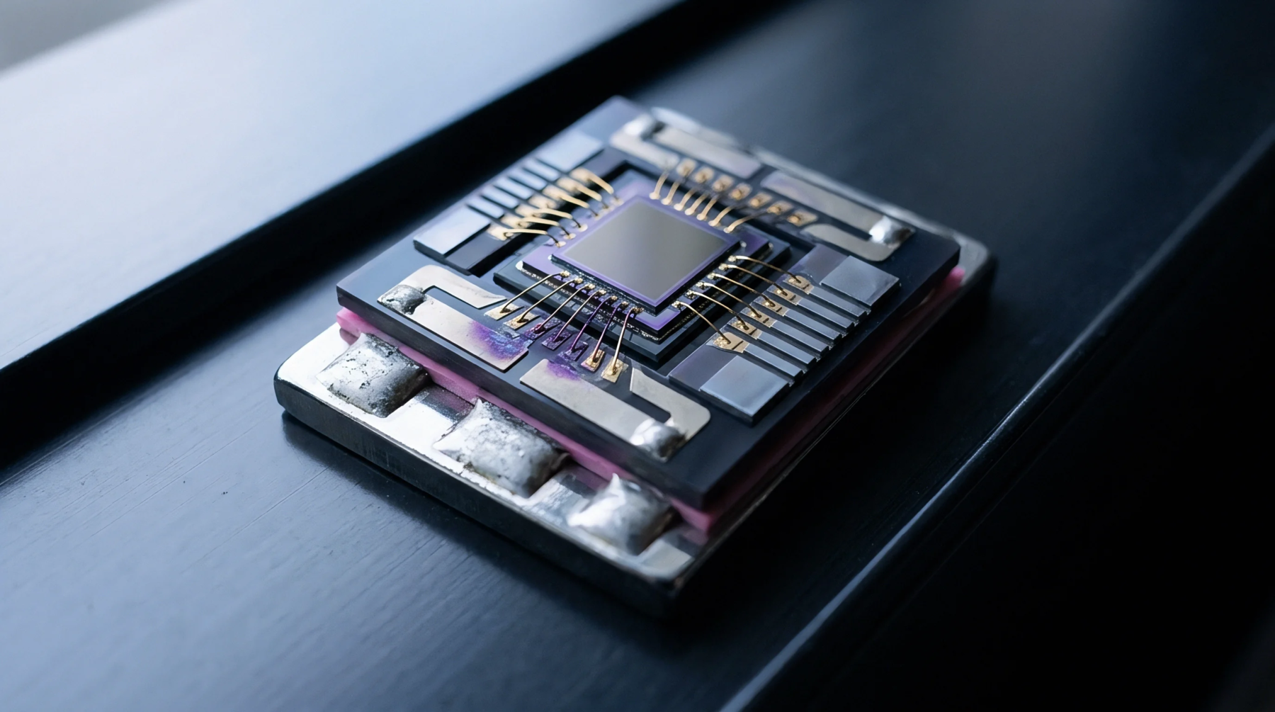
Mechanical contact requires precise alignment between the gull wing leads and the solder paste deposit on the substrate. The tssop relies on these flexible metal pins to absorb thermal expansion coefficients mismatch during operational cycles without fracturing the internal gold wire bonds. Each pin connects to the silicon die through a bonded wire or flip chip bump, creating the electrical link to external signal routing.
Variations in lead coplanarity trigger open circuits during reflow if the deviation exceeds the tolerance set by standard manufacturing guidelines. Inspection protocols use laser profiling to verify that every pin rests within the specified vertical range relative to the seating plane. Adjustments in stencil thickness alter the volume of solder, affecting the fillet shape and long term reliability of the joint under mechanical stress.
Thermal Resistance
Heat dissipation dictates the operational ceiling for this package format. The tssop manages conduction from the silicon junction through the lead frame to the copper traces on the board. Airflow across the surface removes energy, yet the small package volume restricts the rate of convection cooling.
When the internal temperature rises, the signal integrity risks degradation due to increased carrier scattering within the semiconductor material. Designers verify these thresholds using thermal imaging equipment to identify hotspots on the package exterior during peak load conditions. Measurement against a reference temperature confirms the junction to ambient resistance, which quantifies the ability of the enclosure to reject waste heat into the surroundings without failure of the underlying wire connections.
Signal Integrity
High frequency data transmission necessitates minimal parasitic inductance and capacitance within the lead paths. The tssop creates a localized electromagnetic environment where the length of the lead influences the signal propagation delay. Proximity to adjacent pins introduces crosstalk, forcing engineers to isolate sensitive analog inputs from high speed digital outputs.
Calibration of the test fixture ensures that parasitic effects from the socket do not bias the performance data recorded during qualification runs. Frequency response remains stable as long as the ground plane impedance stays low, preventing ground bounce during rapid switching events. Deviations in performance indicate physical degradation of the internal contacts or oxidation of the lead finish.
Proper impedance matching maintains the integrity of transmitted pulses across the entire frequency spectrum of the application.