Die Attach Adhesive Coefficient Mismatch Mitigation in MEMS Accelerometers
Selecting low-modulus die attach adhesives with glass transition temperatures outside operating limits eliminates non-linear MEMS zero-g offset drift.


Shear
Thermomechanical stress inside a sensor package stems from thermal expansion mismatches between the monocrystalline silicon element and the underlying substrate. As operating temperatures change, each layer in the stack expands or contracts according to its atomic lattice. Silicon has a low thermal expansion coefficient, whereas organic circuit substrates, metallic leadframes, and ceramics move much faster.
The die-attach adhesive bridging the chip and substrate absorbs these mismatched dimensional shifts, concentrating mechanical stress around the outer perimeter of the die.
The level of interface force depends on temperature delta, die footprint, and adhesive modulus. In precision micro-electromechanical systems, these forces do not stay isolated at the bond line. The rigid silicon die bows under shear stress, warping dynamically with temperature.
Bending strain propagates upward through the silicon bulk into sensitive micromachined structures on the top surface. In capacitive and piezoresistive accelerometers, this parasitic strain distorts the baseline geometry of suspended proof masses, flexures, and anchors, degrading baseline accuracy before any physical acceleration occurs.

Mismatch Dynamics across Dissimilar Interfaces
Silicon expands at roughly 2.6 parts per million per Kelvin, while standard printed circuit materials expand four to six times faster over industrial operating ranges. When an assembly cools from its high-temperature cure state down to room temperature, the substrate contracts far more than the chip. This differential contraction pulls inward on the bottom surface of the silicon.
The resulting shear stress peaks at the outer edges and corners of the die while remaining near zero at its geometric center.
Stoney’s thin-film relation, adapted for thick die-attach configurations, describes this multi-layer bending behavior mathematically. The radius of curvature varies inversely with the expansion mismatch and the temperature delta relative to the zero-stress curing point. High-modulus adhesives transfer mechanical strain directly into the silicon chip, whereas compliant, low-modulus adhesives absorb dimensional mismatch through internal shear deformation, shielding the element from severe bending moments.
Substrate selection sets the baseline stress environment for the sensor die. Alumina ceramic, expanding at approximately 6.5 to 7.0 parts per million per Kelvin, matches silicon far better than standard FR-4 glass-epoxy composites (14 to 17 parts per million per Kelvin). Copper leadframes present an even larger mismatch at roughly 16.5 parts per million per Kelvin.
Mounting a 3-millimeter square silicon accelerometer directly onto a copper leadframe using rigid conductive epoxy creates interfacial shear stresses exceeding 45 megapascals upon cooling from a 150-degree Celsius cure down to minus 40 degrees Celsius.

Proof Mass Deformation Mechanics
Mechanical strain at the die base travels through the silicon thickness to deform suspended microstructures. In capacitive MEMS accelerometers, proof mass anchors bond directly to the substrate. When shear stress warps the underlying silicon, the distance between adjacent anchors shifts.
This relative movement displaces fixed sense fingers against movable comb fingers attached to the proof mass, shifting nominal capacitance gaps at zero applied acceleration.
A die bow radius of curvature below 1.2 meters induces a zero-g offset drift exceeding 15 millig in a 2-millimeter silicon accelerometer chip subjected to a 100 Kelvin temperature delta.
Piezoresistive MEMS accelerometers show even higher sensitivity to package strain. Piezoresistors diffused or implanted into silicon flexure beams translate deflection into resistance changes. Package-induced strain altering these flexure bridges produces baseline resistance shifts independent of actual motion.
A strain change of just ten microstrain can generate an output shift equivalent to several hundred millig of false acceleration signal.
Asymmetrical adhesive coverage worsens deformation by turning uniform thermal expansion differences into complex warping. Voids, pinholes, or uneven fillets disrupt symmetrical stress distribution across the die base. The resulting strain gradients twist the chip, introducing cross-axis sensitivity errors where primary-axis acceleration registers on an orthogonal channel.
Room-temperature modulus values do not reliably predict package stress, as stiffness can jump by a factor of three once a formulation drops below its glass transition threshold.


Polymer
Die-attach adhesives rely on chemical formulations whose mechanical rigidity varies non-linearly across temperature. Thermosets, silicone elastomers, fluorosilicones, and metal-filled pastes each exhibit distinct molecular behaviors that dictate stress damping. Epoxies remain the standard structural choice due to high bond strength, chemical resistance, and compatibility with automated dispensers.
Unfilled organic resins expand rapidly, often exceeding 50 parts per million per Kelvin; formulators load the matrix with inorganic fillers like fused silica, alumina, or silver particles to bring expansion closer to silicon.
Silicones use a flexible siloxane backbone that yields an elastic modulus two to three orders of magnitude lower than filled epoxies. This extreme compliance allows silicones to shear easily, isolating the silicon chip from substrate movement. Silicones retain flexibility well below minus 50 degrees Celsius.
Though their thermal expansion rates are high ~ typically 150 to 300 parts per million per Kelvin ~ their low modulus keeps actual stress on the die minimal.

Thermomechanical Modulus Behavior across Temperature
Storage stiffness in epoxy drops sharply as thermal kinetic energy crosses the glass transition boundary. Below this threshold, polymer chains remain locked in a glassy state with an elastic modulus between 3 and 10 gigapascals. Above glass transition, thermal energy allows polymer chains to slide, lowering modulus to 50 ~ 300 megapascals while thermal expansion increases by a factor of three to four.
Designing a MEMS die attach with a glass transition temperature inside the operating window introduces severe anomalies. Thermal swings across minus 40 to plus 125 degrees Celsius force the adhesive through its phase transition, driving a non-linear shift in package stress. This sudden change in rigidity shifts the zero-g offset slope during operation, creating an inflection point in thermal drift that standard linear or second-order calibration polynomials cannot compensate for.
Engineers specify formulations with glass transition temperatures well above peak limits (above 150 degrees Celsius) or select compliant systems with transitions well below minimum limits (below minus 60 degrees Celsius).
| Material Chemistry | Elastic Modulus at 25°C (GPa) | CTE Below Tg (ppm/K) | CTE Above Tg (ppm/K) | Glass Transition Tg (°C) | Moisture Absorption (%) |
|---|---|---|---|---|---|
| Silver-Filled Rigid Epoxy | 8.5 | 35 | 120 | 165 | 0.45 |
| Flexible Modified Epoxy | 1.2 | 55 | 160 | 45 | 0.80 |
| Die-Attach Film (DAF) | 3.8 | 40 | 135 | 130 | 0.30 |
| Soft Silicone Elastomer | 0.005 | 180 | 220 | -115 | 0.12 |
| Sintered Silver Paste | 40.0 | 19 | 19 | N/A | 0.02 |

Viscoelastic Relaxation and Moisture Swelling Mechanics
Long-term dimensional drift in organic die bonds stems from physical creep under sustained stress and ambient humidity absorption. Thermosetting polymers exhibit viscoelastic behavior, combining properties of elastic solids and viscous liquids. Under sustained mismatch stress, internal stress within the adhesive gradually relaxes as polymer chains reorient.
This time-dependent relaxation alters die curvature even at static temperatures, causing long-term zero-g bias drift.
Moisture absorption causes additional degradation. Epoxies absorb atmospheric moisture, reaching saturation levels between 0.3 and 1.5 percent by weight depending on chemistry and filler content. Water molecules diffusing into the cross-linked matrix induce hygroscopic swelling, increasing volume and imparting fresh strain on the die base.
Moisture also acts as a plasticizer, lowering glass transition temperatures by up to 20 degrees Celsius and softening the material at elevated temperatures.
- Glass transition crossing alters the material thermal expansion coefficient by a factor of three during operation.
- Viscoelastic stress relaxation causes time-dependent zero-g bias drift under continuous physical strain.
- Hygroscopic lattice expansion introduces parasitic bending moments into the silicon substrate upon moisture exposure.
- Interface delamination localized at die corners creates non-linear thermal hysteresis loops in acceleration readings.
Sintered silver pastes offer an inorganic alternative that avoids viscoelastic relaxation and moisture swelling. Composed of silver particles in an organic binder that burns off during processing, sintered silver forms a dense metallic interdiffusion bond between die back-metal and substrate. The joint delivers high thermal conductivity, an elastic modulus near 40 gigapascals, and a CTE matching silver at 19 parts per million per Kelvin.
Because sintered silver is extremely rigid, substrate stress transfers directly into the silicon die, requiring mechanical decoupling features within the silicon layout.
Selecting an adhesive with a glass transition temperature positioned directly inside the operating temperature range guarantees non-linear bias drift that digital compensation algorithms cannot model.

Offset
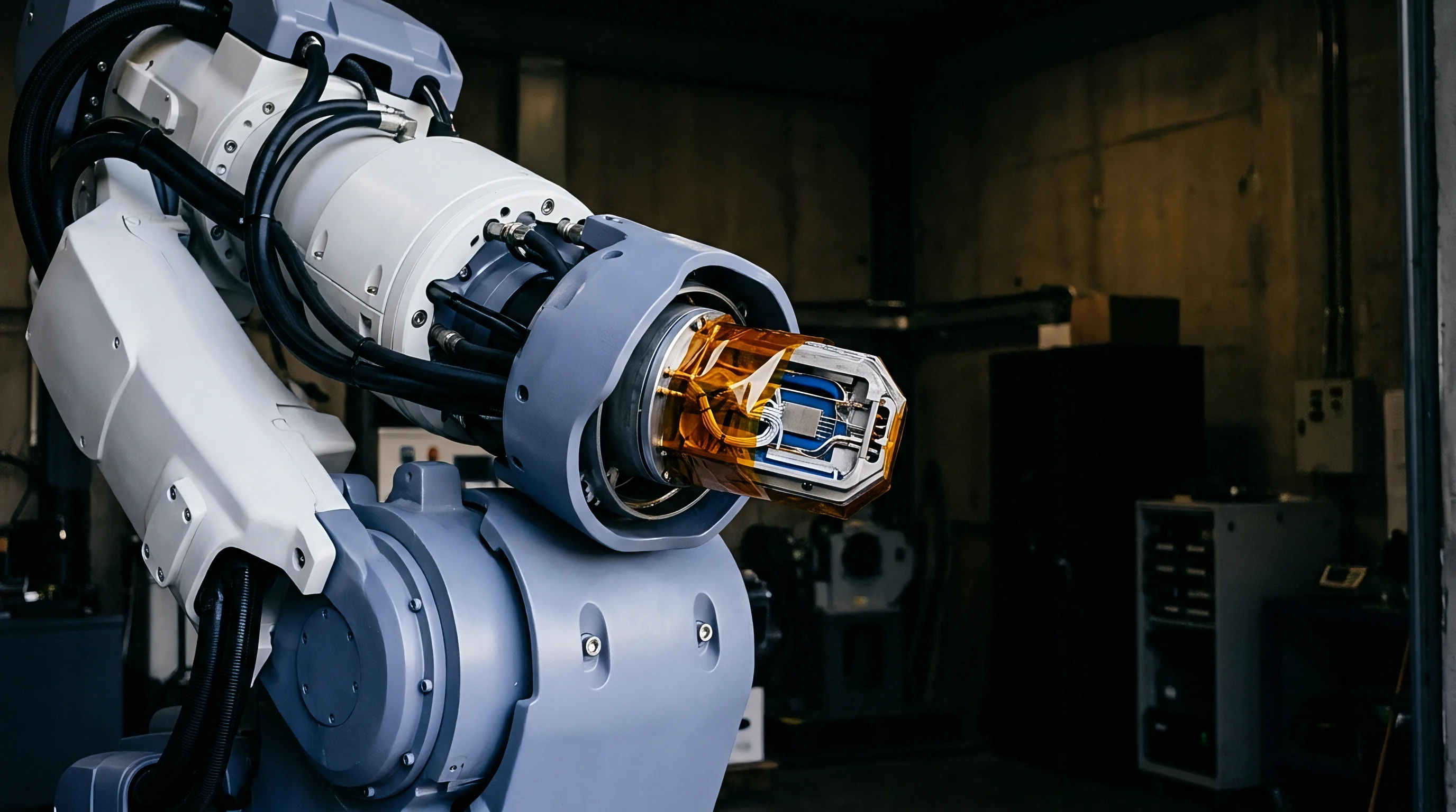
Thermal stress on capacitive sense fingers alters nominal gap spacing between fixed and movable comb structures. In an ideal MEMS accelerometer at zero acceleration, differential capacitance between proof mass fingers and fixed frame fingers stays balanced. When package strain warps the silicon substrate, fixed comb anchors shift by fractions of a nanometer.
With capacitive gap widths measuring 1 to 2 micrometers, an anchor displacement of 0.1 nanometers shifts zero-g output by several millig, setting the baseline Temperature Coefficient of Offset.
Temperature Coefficient of Offset expresses the rate at which zero-g output shifts with ambient temperature, measured in millig per Kelvin or micro-g per Kelvin. Package strain accounts for most non-linear TCO behavior in surface-mount accelerometers. While intrinsic transducing elements show predictable thermal variations that signal conditioning can correct, stress transmitted through die attach varies non-linearly with temperature, producing complex directional strain vectors.

Thermal Hysteresis and Zero Bias Drift Pathways
Temperature swings reconfigure parasitic strain fields within the die bond. When an assembled accelerometer is cycled from room temperature up to plus 125 degrees Celsius and back, zero-g output often fails to return to its initial value. This offset shift defines thermal hysteresis.
Viscoelastic relaxation in epoxy, micro-cracking at die corners, and moisture desorption at high temperatures alter the stress state between heating and cooling legs.
Thermal hysteresis degrades inertial navigation systems that demand high zero-bias stability. A 5-millig hysteresis band invalidates calibrations performed during temperature rise once cooling begins. Rigid epoxy die attach produces wide hysteresis loops that expand with higher peak temperatures and longer dwell times.
Flexible silicones narrow hysteresis substantially, though lower bond strength increases vulnerability to shock and vibration creep.

How Does Glass Transition Temperature Alter Zero Point Bias?
When temperature crosses the glass transition threshold, the thermal expansion slope jumps instantly from a low to a high value, accelerating stress on the silicon die base. The zero-g offset curve forms an inflection point at the glass transition temperature, splitting the thermal profile into two distinct operational regimes with different temperature coefficients.
Modeling this slope shift with standard factory calibration requires high-order math. Standard ASIC architectures use second- or third-order polynomials in non-volatile memory to adjust front-end gain and offset from integrated temperature sensors. When adhesive crosses glass transition, mechanical stress follows a sigmoidal curve that low-order polynomials cannot track, leaving residual offset errors up to 20 millig near the transition point.

Signal Conditioning Limits for Non-Linear Drift
Digital processors use high-order polynomials driven by integrated temperature sensors to compensate for zero-g drift. This compensation assumes the internal diode accurately reflects die-attach temperature and that mechanical stress maps deterministically to temperature without lag or hysteresis. Thermal gradients break the first assumption; viscoelastic creep and hysteresis invalidate the second.
During rapid temperature transients, thermal lag causes internal sense elements and adhesive layers to lag behind temperature sensor readings. The DSP then applies compensation based on an outdated stress state, creating dynamic offset spikes during thermal ramps. Specifying an adhesive without accounting for sub-zero modulus hardening risks field returns from uncompensatable zero-point shifts.
Contract specifications adhering to AEC-Q100 Grade 1 reject accelerometer batches exhibiting zero-g thermal hysteresis greater than 0.5 percent of full-scale measurement range following temperature cycling.

Chamber
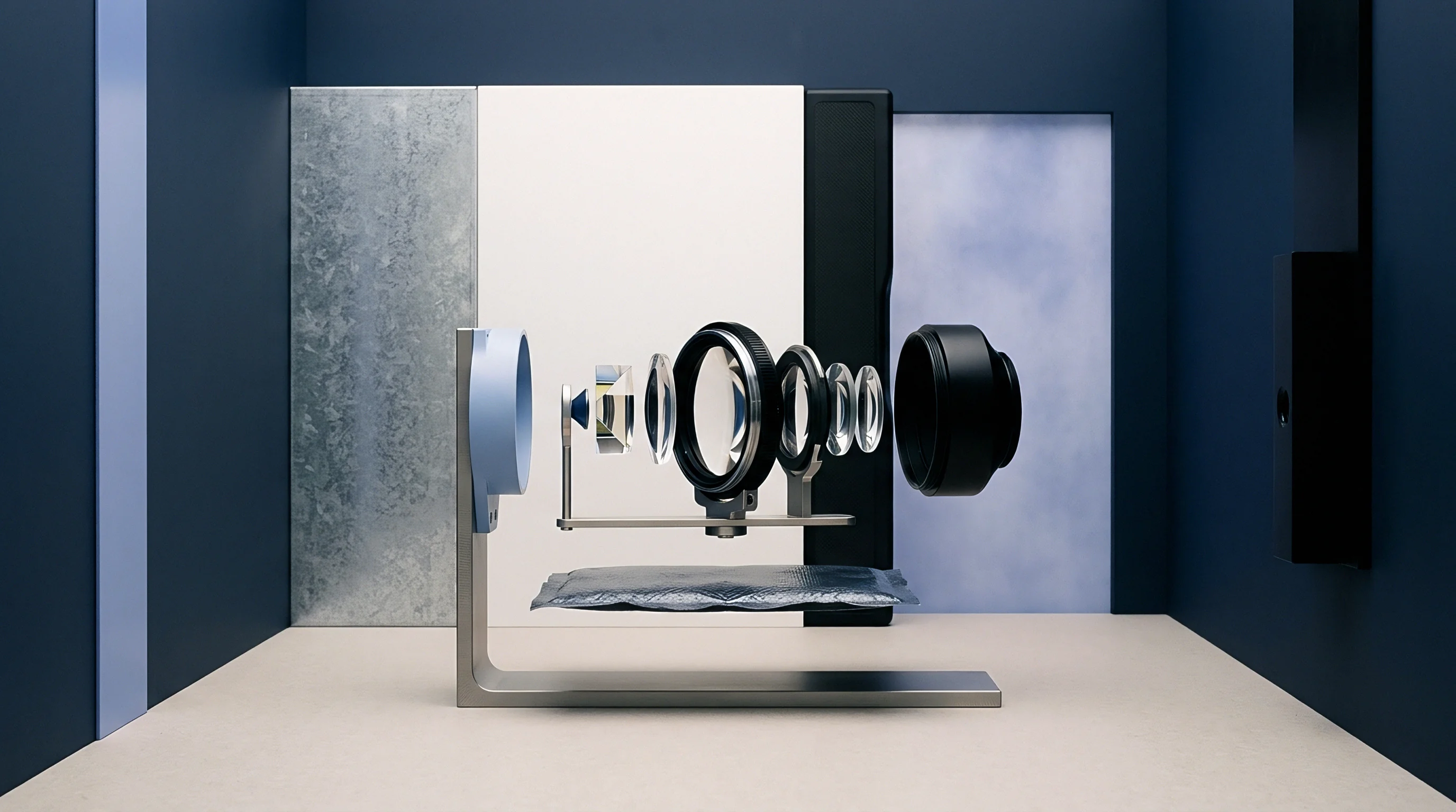
Environmental testing evaluates die bond integrity under accelerated thermal cycling and mechanical shock protocols. Qualification routines simulate years of operational exposure by driving packaged sensors through temperature extremes while tracking deformation, adhesion, and electrical output. Standard chamber runs control ramp rates, dwell times, and relative humidity to isolate structural failure modes.
Engineers monitor zero-g bias drift, cross-axis sensitivity, and delamination to clear designs for volume production.
Accelerated thermal testing targets low-cycle fatigue in die-attach joints. Cyclic expansion differences between substrate and silicon impose shear strains on the adhesive, especially at die boundaries. Over hundreds of cycles, this strain drives micro-voiding and crack propagation in organic matrices, degrading bond strength.
As micro-cracks spread, stress pathways into the silicon shift, causing irreversible baseline calibration drift.

Metrology for Interface Delamination and Die Warpage
Acoustic reflection microscopy detects internal air gaps non-destructively. Focused high-frequency ultrasound (30 MHz to 230 MHz) passes through the silicon chip and reflects off internal interfaces based on acoustic impedance. Solid bonds return a characteristic reflection signature, while air gaps from delamination or voiding reflect nearly 100 percent of incident energy.
Scanning Acoustic Microscopy generates spatial maps showing void locations, edge delamination, and fillet detachment after thermal cycling.
| Standard / Test Method | Environmental Conditions | Test Duration / Cycles | Primary Failure Mode Evaluated | Acceptance Threshold |
|---|---|---|---|---|
| IEC 60068-2-14 Test Nb | -40°C to +125°C, 5°C/min ramp | 500 Thermal Cycles | Low-cycle thermal fatigue, TCO drift | Zero-g offset shift < 5 mg |
| MIL-STD-883 Method 1010 | -55°C to +150°C, air-to-air transition | 100 Thermal Shock Cycles | Interface cracking, severe die tilt | Zero delamination at die corners |
| JEDEC JESD22-A101 | 85°C and 85% Relative Humidity | 1000 Hours Unbiased | Hygroscopic expansion, swelling stress | Sensitivity shift < 0.2% |
| MIL-STD-883 Method 2030 | Acoustic Microscopy (C-SAM) Inspection | Post-Assembly Audit | Adhesive voiding percentage | Total void area < 15% of die area |
| IEC 60068-2-27 Test Ea | 5000 g acceleration, 0.2 ms pulse | 6 Shocks per axis (±X, ±Y, ±Z) | Adhesive shear fracture, die displacement | No mechanical detachment or shift |
Environmental Stress Cycling Protocols
Standard qualification subjects assembled sensors to rapid thermal cycling between minus forty and plus one hundred twenty-five degrees Celsius. Optical shadow moiré and phase-shifting interferometry measure dynamic die warpage inside test chambers with optical viewports. Coherent laser light aimed at the unencapsulated back surface generates interference fringe patterns that map three-dimensional topography with sub-nanometer resolution across thermal sweeps, pinpointing bowing transitions.
- Initial warpage profiling measures baseline silicon chip curvature across room temperature using optical phase-shifting interferometry.
- Acoustic imaging scanning establishes total void percentage and identifies peripheral edge delamination prior to thermal stress exposure.
- Thermal shock exposure subjects test packages to one hundred continuous thermal cycles between environmental extremes.
- Post-stress metrology re-evaluation quantifies changes in die curvature and acoustic void growth across the interface layer.
Applying MIL-STD-883 Method 2030 criteria enforces a 15 percent maximum void area limit to prevent localized stress concentrations that trigger field calibration failures. Void distribution is often more critical than total area: several small central voids totaling 10 percent area rarely impact warpage symmetry, whereas a single contiguous corner void covering 5 percent of die area disrupts symmetry, causing severe cross-axis strain and dynamic tilt errors during thermal swings.


Compliance
Mitigating die-attach stress requires physical isolation features built into the silicon layout and package sub-mount. Rather than relying solely on adhesive compliance, sensor designers build strain relief directly into the assembly structure. Incorporating flexible suspension frames, patterned adhesive footprints, and stress-decoupling silicon interposers isolates sensitive microstructures from package deformation, reducing strain transfer by up to an order of magnitude.
Silicon interposers act as strain buffers between rigid package substrates and active MEMS chips. Matching the interposer CTE to the MEMS die shifts primary thermal expansion mismatch down to the substrate-interposer interface. The die-attach bond between interposer and sensor die sees minimal shear strain over temperature, while a compliant secondary adhesive beneath the interposer absorbs expansion differences relative to the organic substrate.

Structural Stress Isolation and Decoupling Frames
Silicon frames with etched perimeter trenches isolate internal proof mass anchors from package deformation. In standard surface-micromachined layouts, anchors bond directly to the die substrate, moving whenever the substrate bows. Stress-isolated designs etch deep, narrow trenches through the silicon wafer around the central sense element, leaving thin flexure tethers connecting the internal region to the outer die ring.
These silicon flexure tethers act as mechanical low-pass filters for package strain. When thermal stress warps the outer die ring, the compliant tethers deform, absorbing physical displacement before strain reaches central anchors. Test data confirms that central single-anchor layouts with perimeter relief trenches reduce zero-g offset thermal sensitivity by over 80 percent compared to four-corner anchor configurations on continuous substrates.
- Centralized dot dispense restricts adhesive footprint to thirty percent of die surface area, reducing perimeter strain transfer.
- Precision spacer bead integration maintains a uniform bond line thickness of thirty-five micrometers to distribute shear loads evenly.
- Silicon interposer sub-mounts match chip expansion coefficients to buffer rigid substrate movements before reaching microstructures.
- Relief trench etched anchors decouple the capacitive comb anchor points from outer die substrate warpage.

Adhesive Geometry Optimization and Dispense Architecture
Patterning liquid adhesive into discrete cross or five-dot matrix shapes provides expansion relief during thermal swings. Standard assembly lines often dispense a single central drop, pressing the chip to squeeze adhesive out to die edges. Full-coverage bonds maximize thermal shear transfer across the die, driving up warpage.
Multi-dot patterns leave unbonded channels where the polymer can expand horizontally into open relief space without imparting stress to the silicon.
Controlling Bond Line Thickness ensures uniform stress distribution across the die attach. Thin adhesive layers below 10 micrometers increase shear stress sharply, as shear strain scales inversely with bond line thickness. Increasing thickness to 30 ~ 50 micrometers provides a compliant cushion that distributes shear deformation, reducing net bending moments on the silicon.
Precision packaging blends tightly graded glass spacer beads (typically 35 micrometers in diameter) into adhesive formulations at 1 ~ 2 percent weight concentrations to ensure uniform, repeatable bond line height in mass production.
A central anchor design reduces thermomechanical stress transfer to sensing microstructures by up to eighty percent compared to four-corner die bonding architectures.
Die Attach Film (DAF) offers an alternative to liquid pastes, providing uniform bond line thickness and eliminating squeeze-out variations. DAF consists of epoxy film pre-laminated to the wafer backside before dicing. During placement, the film cuts cleanly along die edges, ensuring 100 percent coverage without fillet creep.
While DAF ensures uniform thickness, its high elastic modulus and full coverage generate substantial shear stress, requiring internal decoupling trenches to limit zero-g offset drift. Whether film adhesives can achieve the low modulus needed for precision inertial sensors without long-term outgassing risks remains an active technical debate.

Yield
Commercial viability requires balancing low-stress adhesive chemistry against production throughput and supply chain stability. Selecting a die attach involves trade-offs between elastic modulus, cure speed, shelf life, thermal conductivity, and material cost. Soft silicone adhesives isolate package stress effectively, but low shear strength reduces yield during automated wire bonding, where ultrasonic energy requires a rigid die base.
High-modulus epoxies enable fast wire bonding and sub-60-second snap cures, but generate high thermomechanical stress that increases scrap rates during precision calibration.
Sourcing engineers evaluate unit material price against total landed manufacturing cost. Specialized low-stress epoxies and high-purity siloxanes carry high price tags, often exceeding two thousand dollars per kilogram. Because a 3-millimeter MEMS accelerometer requires under 0.2 milligrams of adhesive per package, raw material cost per unit remains below a fraction of a cent.
Scrap costs from calibration failures represent the real financial driver; a 1.5 percent increase in zero-g offset failure rate during burn-in testing costs far more than upgrading to a premium low-stress formulation.

Supply Chain Dynamics and Storage Logistics
Advanced die-attach epoxies require continuous sub-zero shipping and storage to prevent premature curing. Premixed frozen syringes represent the standard delivery method for high-reliability pastes. Formulators package blended resins into single-use syringes, purge them with nitrogen to remove micro-bubbles, and blast-freeze them to minus 40 degrees Celsius to halt chemical reaction kinetics.
Cold-chain logistics with continuous temperature logging ensure the material never warms above minus 40 degrees Celsius prior to reaching the dispense line.
Storage management directly impacts assembly yield and dispense accuracy. Premixed frozen epoxies have strict shelf limits, typically six months at minus 40 degrees Celsius. Once removed from storage, syringes require a controlled room-temperature thaw (typically 45 to 60 minutes) to reach thermal equilibrium without moisture condensation on syringe walls.
Thawed work life spans 8 to 24 hours depending on the catalyst. Exceeding work life leads to solvent evaporation and ambient cross-linking, increasing viscosity and altering dispense dot volume, which disrupts bond line thickness uniformity across production lots.

Material Qualification and Dual-Source Protocols
Re-qualifying an alternate die-attach formulation requires six months of environmental testing and extensive recalibration of ASIC thermal compensation tables. Qualifying a secondary adhesive vendor involves far more than comparing datasheet properties. Subtle shifts in resin cross-linking density, filler particle size distribution, or trace solvent content alter viscoelastic relaxation rates and temperature-dependent modulus slopes, changing the thermal drift profile of the package.
| Manufacturer / Product Line | Chemistry Class | Primary Market Focus | Storage Requirements | Work Life at 25°C | Relative Unit Cost |
|---|---|---|---|---|---|
| Henkel LOCTITE ABLESTIK 84-1LMSR | Silver-Filled Conductive Epoxy | Automotive Inertial / AEC-Q100 | -40°C Cold Chain | 18 Hours | Moderate |
| Namics CHIPCOAT ME-8451 Series | Silica-Filled Low-Stress Epoxy | High-Precision Industrial MEMS | -40°C Cold Chain | 12 Hours | High |
| Dow SILGARD 6611 Silicone Elastomer | Compliant Siloxane Gel | Extreme Thermal Range Sensors | Room Temperature (<25°C) | 24 Hours | Moderate |
| Shin-Etsu KER-3000 Series | Optoelectronic / Sensor Silicone | Consumer & Industrial Inertial | Two-Part Mix at Line | 72 Hours Mixed | Low |
| MacDermid Alpha Argomax Sintered Ag | Nanoscale Silver Paste | Ultra-Reliability Harsh Environment | -20°C Cold Chain | 8 Hours | Very High |
Securing dual-source approval requires running parallel environmental qualification lots through full IEC 60068 thermal cycling schedules while collecting high-volume TCO data across multiple wafer lots. Assembly plants establish strict incoming quality audits measuring viscosity, gel time, outgassing percentage, and silver filler settling rates for every paste lot before release to automated dispense lines. Maintaining dual-sourced materials with matching viscoelastic properties protects production lines against supply allocation notices while keeping long-term calibration drift within specification.