
Supply Allocation Exposure across Dual Sourced Low Tier Commercial Sensor Topologies
Dual sourcing low tier commercial sensors demands matching ASIC DSP group delays and thermal offset drift profiles to prevent host control loop instability.
Dual sourcing low tier commercial sensors demands matching ASIC DSP group delays and thermal offset drift profiles to prevent host control loop instability.

Hierarchical I2C switches isolate bus capacitance and expand address space while adding measurable transaction delays and timing limits that firmware state machines govern.
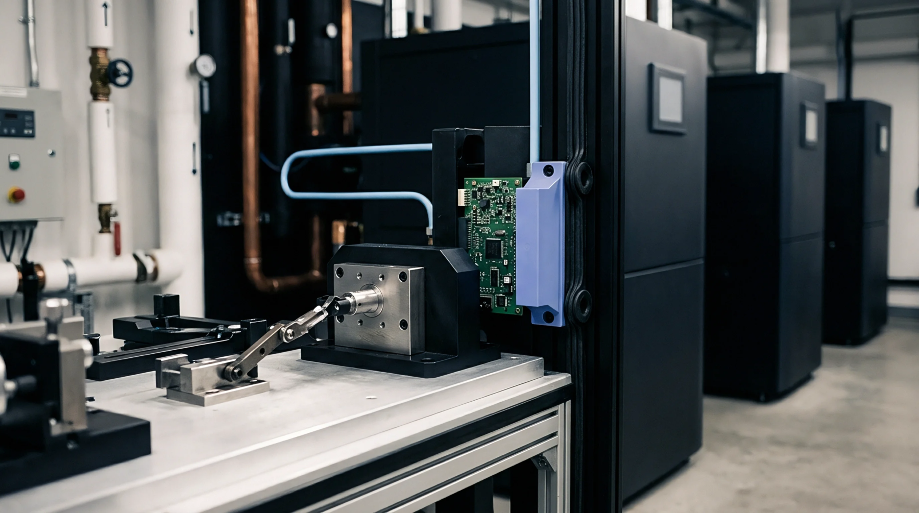
Active guard architectures require closed loop phase alignment below 0.05 degrees to eliminate moisture induced stray capacitive leakage currents.
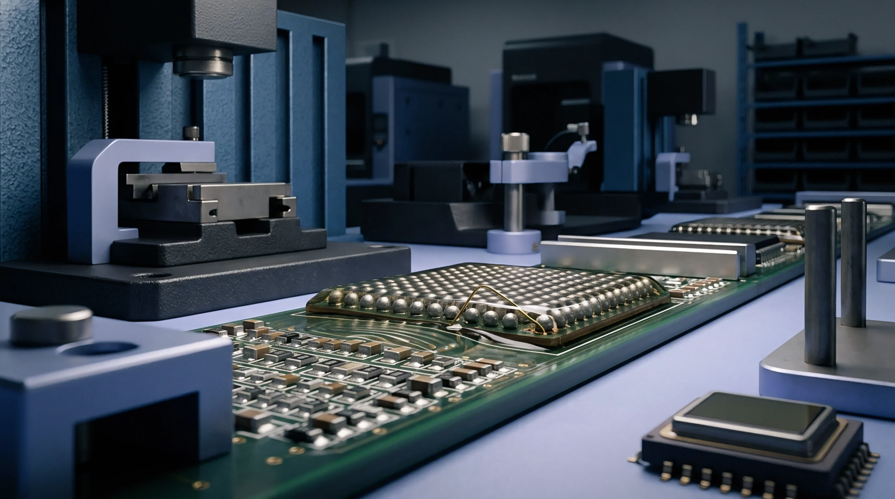
Calculated land pattern dimensions matching IPC-7351 guidelines balance solder fillet volume and placement tolerance to prevent joint stress and yield loss.

CMOS image sensor row readout delay dictates rolling shutter temporal skew, determined by physical word line RC delays and column ADC settling times.

Active buffers isolate bus capacitance beyond 400 picofarads by segmenting traces and using static voltage offsets or edge accelerators to meet timing limits.

Multi-channel sensor integration on standard two-wire buses demands balancing parasitic bus capacitance, address resolution, layout geometry, and landed unit cost.
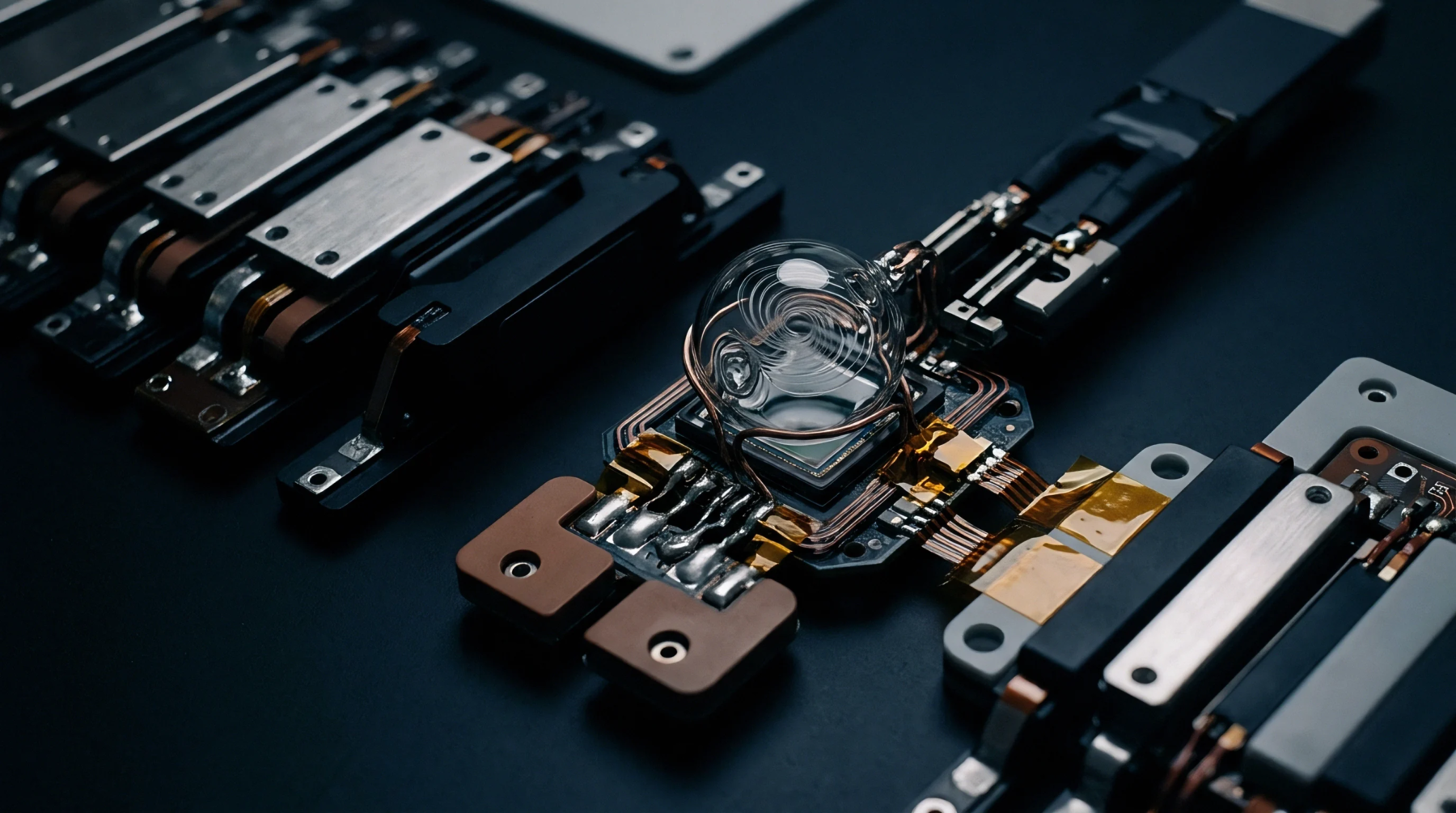
Dynamic address assignment eliminates external multiplexers in dense sensor arrays, trading minor firmware development time for reduced PCB routing and lower bill-of-materials costs.
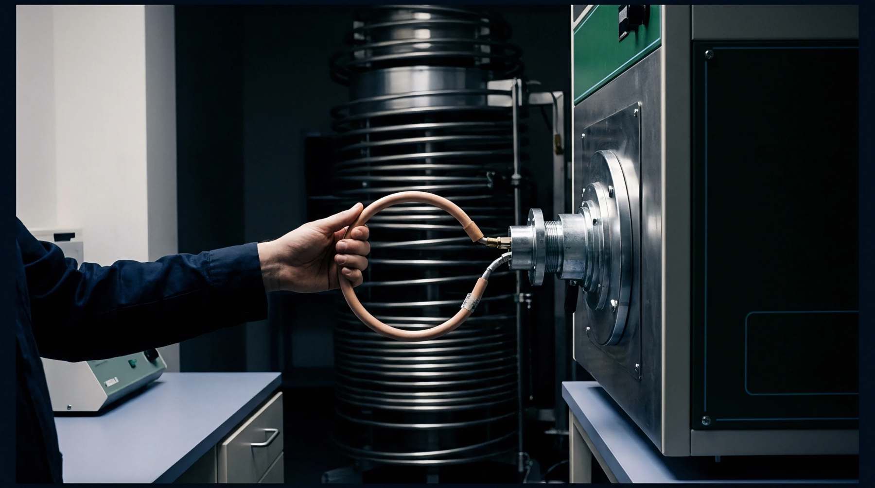
Selecting sensor packages and digital interfaces balances bus trace capacitance, pull-up current, thermal assembly stress, and firmware driver maintenance costs.

Reconfigurable front ends bridge piezoelectric charge and piezoresistive voltage modalities by actively commuting amplifier loops and parasitic switch nodes.
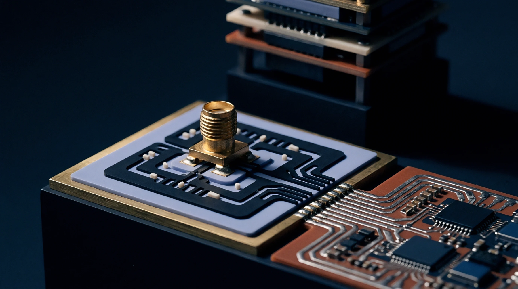
Determining clock low bounds across thermal cycles requires evaluating internal oscillator drift, package piezoresistive strain, and supply rail variations.

Baseline capacitance drops during evacuation due to gas density loss, surface moisture desorption, and elastic housing deformation under vacuum pressure.

Modelling QFN land pattern parasitics balances via inductance, standoff capacitance, and substrate dielectric choices to maintain high-speed interface signal integrity.

Active driven shielding neutralizes cable capacitance and fringe fields by holding an intermediate guard conductor at identical instantaneous sensor potential.

IEEE 1838 die register verification across high-density interposer bumps requires cycle-accurate scan patterns mapped to low-skew DWR and FSI boundary registers.

Non-equilibrium microstructural evolution in silicon suspension beams drives mechanical quadrature drift beyond transimpedance amplifier saturation ceilings.

Match physical transduction mechanisms to target material limits, thermal loop expansion, and analog noise ceilings before selecting specific sensor vendors.
Dynamic bus segmentation isolates faulted branches with analog switches while nine-pulse clock sequences and high-side FET resets clear locked slave logic.
Resolve translator timing degradation by segmenting bus capacitance below eighty picofarads, adding series damping, and disabling one-shot accelerators.

Ambient moisture absorption into plastic packaging drives mechanical swelling strain, inducing uncalibrated offset drift and sensitivity shifts in MEMS dies.

Line readout delay is the sequential horizontal row digitization time governing progressive CMOS exposure skew, image shear, and motion blur geometry.

Distributed interconnect parasitic capacitance limits row line switching speed, demanding full 3D extraction to prevent array settling errors.

Silanol condensation releases cavity water that shifts internal permittivity, demanding high-temperature bakeout or atomic layer deposition to lock dielectric drift.
Cascade multi-tier buses by matching loaded line impedances and limiting physical stub lengths to under one-third of the signal edge transition length.

Dynamic bus capacitance equals host load plus off-state switch parasitics and active segment trace and pin loads across operational state combinations.
Clock stretching allows open-drain targets to hold SCL low, forcing host timing compliance through physical line sensing and hardware timeouts.

Silicon stepping registers provide unambiguous hardware verification, ensuring firmware driver compatibility and protecting production lines from unannounced die alterations.

Transfer molding stresses deform transducer diaphragms, shifting zero-point calibration by up to three percent full scale across reflow assembly cycles.

Complex impedance tracking decomposes inductive coil signals into resistance and reactance to decouple physical displacement from target conductivity and temperature.

Solder voids over twelve percent under differential signal ground returns introduce local impedance drops that erode multigigabit channel margins.
Expertise is a utility, not a secret. sentiention™ publishes its working knowledge as open reference: intelligence layer covering the materials it sources, the markets it enters, and the reference that serves both.