Fundamentals of Driven Shielding for Capacitive Displacement Sensors
Active driven shielding neutralizes cable capacitance and fringe fields by holding an intermediate guard conductor at identical instantaneous sensor potential.


Guard
A capacitive sensing node delivers approximately 1.2 picofarads of displacement capacitance across a 100-micrometer measurement gap when excited by a 100-kilohertz sinusoidal carrier. Connecting that electrode to remote signal electronics through one meter of conventional RG-178 coaxial cable places 95 picofarads of shunt capacitance directly across the sensing terminal. That parasitic path diverts over ninety-eight percent of the displacement current straight into the ground reference before the front-end transimpedance amplifier can register the charge.
The nominal gap reactance of 1.33 megaohms drops into an effective parallel load of 16.7 kilohms, collapsing sensitivity and rendering sub-nanometer resolution impossible.
Surrounding the high-impedance sensing electrode with an intermediate conductive shell maintained at an identical instantaneous alternating potential neutralizes this charge leakage. Because the potential difference between the measurement electrode and this intermediate conductor remains at zero volts throughout the AC excitation cycle, the displacement current across the intervening dielectric vanishes according to the differential form of Gauss’s law. Active guarding forces the electric field between the center conductor and the shield to collapse.
The parasitic capacitance continues to exist as a physical property of the cable and housing geometry, yet it conducts zero displacement current because the alternating voltage drop across it equals zero.
Equipotential shielding drives parasitic capacitance toward zero by eliminating the voltage gradient across boundary conductors.
The external shield wraps around this intermediate conductor and connects directly to the instrument chassis ground. While the sensing node sees zero voltage drop to the driven shield, the driven shield swings against the outer ground shield, bearing the entire charging current of the cable capacitance. A low-impedance voltage buffer drives this charging current, isolating the femtofarad-level sensing electrode from the heavy reactive load of the harness.
Cable movement alters the capacitance between the driven shield and outer ground, yet that alteration loads only the operational buffer output stage rather than the sensitive displacement charge collector.
Physical construction demands rigorous concentricity. Probe heads utilize a central measurement electrode, an annular guard ring separated by a sub-millimeter insulating gap, and an outer grounded housing. PEEK, sapphire, and alumina serve as typical structural insulators between these concentric metals.
The sensing electrode diameter determines the measurement spot size, while the guard ring outer diameter sets the boundary conditions that eliminate fringe field curvature across the sensing area. The driven shield extends from the probe face, through the connector backshell, down the intermediate braid of a triaxial cable, and terminates at the low-impedance output pin of the active guard driver.
Matching the guard potential to the sensor node within sub-millivolt precision preserves charge linearity across wide dynamic ranges.


Buffer
Operational amplifiers tasked with driving the intermediate shield encounter severe reactive loading. Driving one to three meters of triaxial cable presents between 100 and 350 picofarads of capacitance directly to the buffer output terminal. This capacitive load interacts with the amplifier open-loop output resistance, inserting an unintended pole into the feedback loop transfer function.
The resulting phase lag erodes phase margin, creating peaking in the frequency response, severe overshoot, or sustained megahertz oscillation that injects broad-spectrum noise into the displacement measurement channel.

Is Active Bootstrapping Stable under Reactive Loading?
Maintaining closed-loop stability across variable cable lengths demands isolation between the output stage and the reactive load. Placing a small series resistor inside the feedback loop, or employing specialized operational amplifiers stable into infinite capacitive loads, prevents phase erosion. The unity-gain driver must track the excitation carrier with negligible phase delay and near-zero amplitude attenuation.
A phase lag of merely 0.5 degrees between the sensing electrode and the driven shield reintroduces a differential voltage vector across the stray capacitance, causing the effective input capacitance to rebound from near-zero to several picofarads.
| Topology | Input Capacitance | Slew Rate | Gain Bandwidth | Phase Delay | Effective Guard Error |
|---|---|---|---|---|---|
| Bipolar Unity Follower | 3.5 pF | 20 V/µs | 15 MHz | 2.40 deg | 4.18 pF |
| JFET Input Buffer | 1.2 pF | 45 V/µs | 35 MHz | 0.35 deg | 0.61 pF |
| CMOS Rail-to-Rail | 4.8 pF | 12 V/µs | 10 MHz | 3.60 deg | 6.28 pF |
| Discrete Composite JFET | 0.4 pF | 180 V/µs | 120 MHz | 0.08 deg | 0.14 pF |
Phase matching represents the defining performance metric of the shield driver. High-speed precision systems often bypass standard operational amplifiers in favor of dedicated bootstrap circuits utilizing matched dual JFETs operating in source-follower arrangements. The source follower presents an input capacitance below 0.5 picofarads, introduces negligible phase shift at carrier frequencies up to 500 kilohertz, and supplies sufficient current to drive several hundred picofarads of cable capacitance without thermal strain.
A buffer voltage offset of two millivolts produces forty picofarads of equivalent stray capacitive error when modulating across a ten-volt sensor excitation span at one hundred kilohertz.
Instabilities in the active guard loop manifest in distinct failure modes that degrade position resolution:
- High-frequency ringing produces wideband spectral sidebands around the carrier tone, inflating the displacement noise floor by twenty to forty decibels.
- Thermal offset drift alters the direct-current potential difference across board-level guard traces, generating picoampere leakage currents across surface contaminants that register as slow position drift.
- Slew rate saturation occurs during high-amplitude carrier excursions, clipping the guard waveform and creating severe harmonic distortion in synchronous demodulator stages.
- Capacitive peaking amplifies out-of-band environmental noise, causing the probe to pick up external switch-mode power supply emissions through the imperfectly guarded sensor rim.
What remains undetermined is whether composite discrete-monolithic driver architectures can maintain sub-zero-point-one degree phase alignment across wide industrial operating envelopes spanning negative forty to eighty-five degrees Celsius without active temperature control.

Fringe
Electric flux lines departing a bare disk conductor spread laterally into space before terminating on an opposing conductive plane. This expansion inflates the measured capacitance above the theoretical parallel-plate equation value calculated from plate area and separation distance alone. In unshielded probes, this lateral spread alters the effective sensing area as the probe retracts from the target, introducing pronounced non-linearity into the displacement calibration curve and increasing susceptibility to lateral target geometry shifts.
Geometric Guard Ratio and Standoff Limits
Surrounding the active sensor disk with an equipotential guard ring of identical surface elevation forces the electric field directly beneath the sensing electrode into straight, parallel lines. The fringing field still exists, but it forms exclusively between the outer boundary of the guard ring and the target. The sensing electrode captures only the uniform, homogeneous field region.
The ideal relationship between the guard ring width and the maximum measurement standoff distance defines whether edge fringing distorts the sensor linearity.
Planar guard rings suppress edge fringing by establishing parallel electric field lines directly perpendicular to the target surface.
Finite element calculations and empirical testing establish clear criteria for guard geometry. For a sensing electrode of radius r operating at a standoff distance d, the annular guard ring width w must equal or exceed three times the maximum standoff distance to achieve non-linearity errors below 0.05 percent. When the standoff exceeds one-third of the guard width, fringe fields bend across the insulating boundary between the guard and sensing electrode, corrupting the measurement current.
Designing guard electrodes requires balancing physical envelope constraints against measurement fidelity:
- Guard ring width must span at least three times the maximum operating gap distance to isolate the central sensing area from bending edge flux lines.
- Insulation trench width between guard and sensor must remain below twenty-five micrometers to prevent significant field penetration into the dielectric substrate.
- Surface coplanarity across the guard and sensor face must stay within one hundred nanometers to avoid creating localized electrostatic field distortions.
- Target target lateral dimension must extend past the outer perimeter of the guard ring by at least two times the measurement standoff distance.
Omitting the planar guard ring increases cross-axis tilt sensitivity by over eight hundred percent, causing micro-radian angular misalignments to register as micrometers of false linear displacement.

Harness
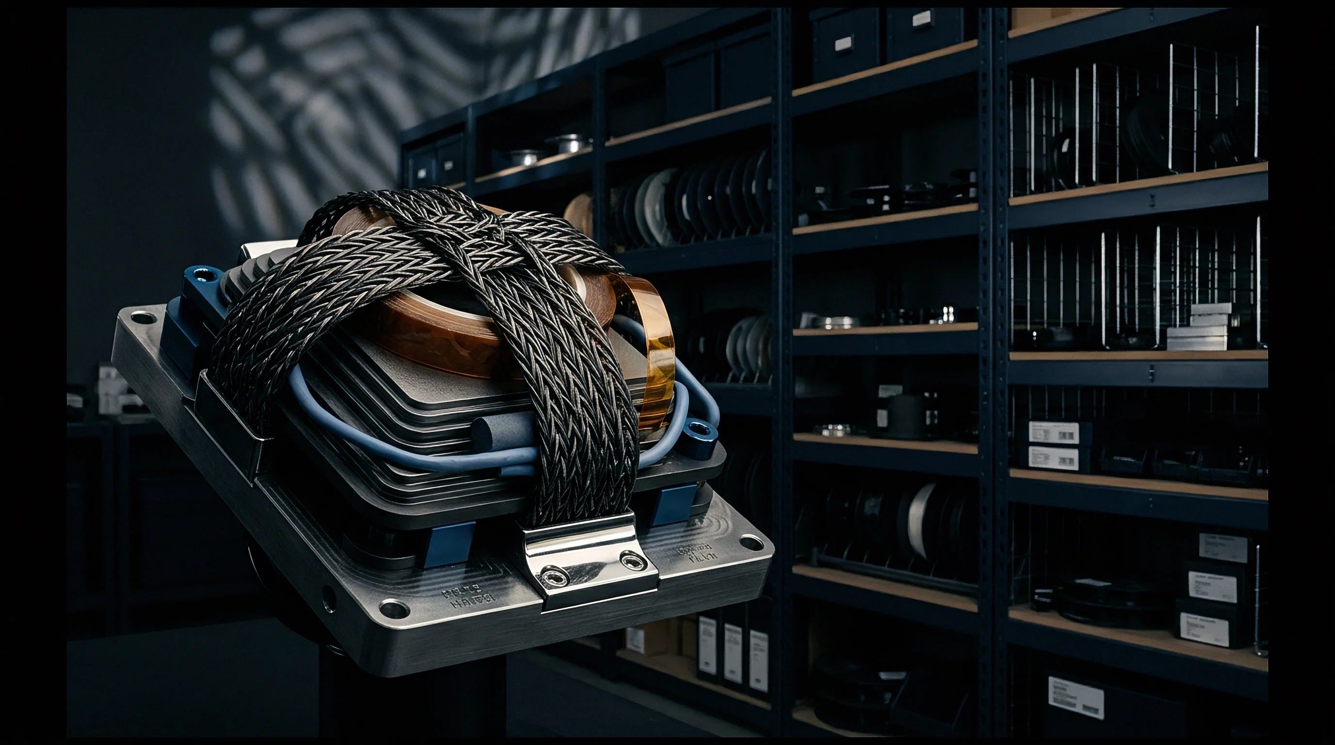
Transmission of picoampere displacement currents over physical distances requires specialized cabling architectures. A standard coaxial cable features a single center conductor surrounded by a grounded dielectric braid. In an actively shielded system, that architecture proves inadequate because grounding the braid re-establishes the full cable shunt capacitance.
Systems must deploy triaxial cabling featuring a center conductor, an inner driven shield braid, an intermediate dielectric layer, an outer grounded shield braid, and an outer protective jacket.

Are Cable Reflections Limiting Transconductance Bandwidth?
Signal propagation along a transmission line encounters characteristic impedance boundaries. At 100 kilohertz carrier frequencies, a two-meter cable represents an electrically short line where lumped-element models apply. However, higher-order harmonics generated by square-wave switching excitation or megahertz-band RF carriers transform the harness into a distributed transmission line.
Characteristic impedances of miniature triaxial cables range between 30 and 75 ohms. Impedance mismatches between the probe head and the amplifier termination cause voltage wave reflections that alter the apparent phase between the center conductor and the driven shield.
| Dielectric Material | Dielectric Constant | Dissipation Factor (100 kHz) | Triboelectric Noise | Flex Fatigue Life |
|---|---|---|---|---|
| Solid PTFE | 2.05 | 0.0002 | Moderate (35 pC/N) | 500,000 cycles |
| Expanded PTFE | 1.30 | 0.0001 | Low (12 pC/N) | 2,000,000 cycles |
| Fluorinated Ethylene Propylene | 2.10 | 0.0003 | High (65 pC/N) | 250,000 cycles |
| Graphite-Coated Polyethylene | 2.25 | 0.0008 | Ultra-Low (2 pC/N) | 1,000,000 cycles |
Mechanical flexure of the sensor harness introduces triboelectric charge. Friction between the dielectric insulator and the braided shields strips electrons, creating charge spikes that flow directly into the ultra-high impedance measurement node. Low-noise triaxial cable incorporates a conductive carbon-doped thermoplastic or graphite coating between the dielectric layers and the copper braid.
This semi-conductive interface discharges frictional charge accumulation safely into the driven shield before it reaches the central signal conductor.
Harness termination demands a strict assembly sequence to preserve active shield integrity:
- Strip the outer jacket and comb the outer ground braid into a single pigtail for chassis bonding.
- Score the intermediate dielectric without cutting the inner shield braid to prevent localized capacitive imbalance.
- Connect the inner shield braid circumferentially around 360 degrees to the intermediate connector backshell.
- Strip the inner dielectric to expose the center conductor while ensuring zero contact with conductive graphite residue.
- Insulate the signal pin termination with high-resistivity cross-linked polyolefin heat shrink to resist moisture absorption.
When sub-nanometer position jumps appear on a bench setup during routine room temperature cycling, cable assembly technicians often claim that small variations in connector crimp torque between batches have no measurable effect on the guard drive capacitance balance.

Margin
Capacitive displacement sensors deliver linear accuracy only when electronic, mechanical, and environmental boundaries remain balanced. Sourcing teams reviewing sensor quotations frequently discover wide price disparities between probes sharing identical stroke lengths and nominal resolution figures. The divergence traces back to internal guarding topology, temperature compensation, and assembly tolerances within the front-end probe housing.
Low-cost probes eliminate active guard rings in favor of passive ground shields, transferring the burden of edge-effect linearization to lookup tables stored in host processor memory.
Firmware-based linearization schemes fail when the target moves laterally or tilts relative to the probe face. Because passive shielding leaves fringing fields unconfined, shifts in target surface topography alter the non-linear transfer function dynamically. A true actively guarded sensor preserves an absolute spatial calibration geometry, maintaining measurement accuracy across varying target profiles and tilt angles up to several degrees.
Verifying sensor performance requires procurement dossiers to mandate full-chain calibration certificates covering both static gap sweeps and dynamic tilt variations.
Specifying calibration compliance under IEC 61326-1 annex A binds the supplier to full-scale drift limits during active radio-frequency field exposure.
Cable lengths represent a rigid contractual constraint in precision capacitive displacement procurement. Capacitive probes cannot undergo field cable trimming or field extension without invalidating factory calibration. The phase adjustment, driver damping resistance, and frequency response of the active guard buffer align with the specific capacitance and propagation delay of the cable harness delivered in the box.
Cutting fifty centimeters from a triaxial harness increases buffer damping ratio, shifts the carrier phase margin, and alters the displacement scaling factor by several tenths of a percent.
Every commercial sensor agreement must reference standard testing protocols to avoid ambiguous warranty disputes. Section 6.2 of the procurement specification stipulates that total measurement error across the rated temperature window shall include cable flexure noise and driven-shield phase lead error, rendering lots with uncompensated harness terminations subject to immediate rejection at incoming inspection.