Spatial Thermal Gradient Effects on Differential Capacitive Sensors
Spatial thermal gradients alter capacitive electrode gaps unevenly, breaking mechanical symmetry and generating uncompensated offset drift in differential sensors.


Plate

Differential Spatial Physics and Common Mode Breakdown
Differential capacitive transducers rely on structural symmetry to reject environmental disturbances. Uniform ambient temperature shifts expand both gaps equally and change the permittivity of the cavity gas at identical rates. Subtracting baseline capacitance across the two electrode pairs cancels those common-mode effects, preserving the true displacement measurement.
But that balance collapses once directional heat flux traverses the package: a temperature differential across opposing plates warps the physical geometry of one side relative to the other, generating an offset indistinguishable from an applied mechanical load.
For parallel plates separated by nominal gap d0, baseline capacitance depends on electrode area A and medium permittivity varε. Applying displacement x widens one gap to d0 + x and narrows the opposite to d0 – x, yielding a normalized capacitance difference:
fracΔ CC0 = fracC1 – C2C1 + C2 = fracxd0
When an internal component or external boundary condition imposes a spatial gradient nabla T across the assembly, electrode temperatures diverge by Δ Tspatial. Structural expansion governed by the substrate mount’s coefficient of thermal expansion α widens the warmer gap to d1 = d0 (1 + α T1). At the same time, cavity gas permittivity shifts according to its temperature coefficient β = frac1varεfracpartial varεpartial T. The perturbed differential ratio becomes:
fracΔ CC0 ≈ fracxd0 + frac12left( α + β right) Δ Tspatial
A spatial difference of 0.1 Kelvin across a 2-millimeter MEMS die with a 1.5-micrometer nominal gap induces a differential capacitance shift of approximately 0.15 femtofarads. In high-precision capacitive accelerometers or inclination sensors with 100 femtofarads full-scale spans, that imbalance drains 0.15 percent of full scale per tenth of a degree of cross-die divergence. Bulk compensation schemes cannot catch the drift; external thermistors track mean die temperature rather than the slope across it.
Spatial gradient drift scales directly with substrate thermal resistance, turning a 0.1 Kelvin cross-die temperature difference into a 0.15 percent full-scale measurement error.
Mechanical Strain Coupling in Asymmetric Thermal Fields
Uneven heating drives mechanical strain as well as localized expansion. As silicon substrates and glass-ceramic headers expand non-uniformly across their lateral dimensions, shear stresses build along the bondline between the die attach adhesive and the package floor. That shear deflects the cantilevered or perimeter-clamped proof mass, pulling the movable electrode out of parallel alignment.
Even tilts below 10 microradians distort the capacitive field between the rigid stators and the suspended rotor. As fringe fields at the plate edges lose symmetry, the electrical centroid pulls away from the geometric center. Bridge drive topologies assume equal current division under symmetric excitation voltages; edge field asymmetry breaks that balance, injecting out-of-phase quadrature currents into the front-end charge amplifier that downstream synchronous demodulators cannot reject.
Whether advanced isotropic packaging materials can fully decouple micro-machined sensing elements from structural warping during dynamic warm-up cycles remains an open question.

Conduction
Heat Transfer Paths across Sensor Elements
Heat enters the sensor package through three routes: conduction via pins and die attach, convection through internal cavity gas, and radiation from nearby dissipation sources. Conduction along PCB traces dominates thermal transients. Regulators, power stages, and microcontrollers routed close to the sensor dump energy into common planes, driving lateral heat fluxes directly into the mounting pads.
When silver-filled epoxy layers beneath the die contain air pockets or vary in bondline thickness, heat flows into the silicon substrate asymmetrically. Portions of the die resting on continuous epoxy conduct far faster than sections suspended over voids. Thermal equilibrium between opposing plates then stretches from milliseconds out to seconds, dragging out transient measurement errors.
The fill gas introduces a secondary transport mechanism. Cavities sealed with dry nitrogen or argon at atmospheric pressure transfer heat between the package lid and internal silicon features through molecular conduction. In low-g accelerometers and differential pressure sensors with taller cavity profiles, steep vertical gradients can also induce natural convection, depositing heat unevenly across the upper plate faces.
- Die Attach Voiding causes localized thermal bottlenecks that slow temperature equalization across opposing differential capacitor arms.
- Asymmetric PCB Copper Routing creates unbalanced conduction channels into grounding pins, establishing steady-state lateral gradients.
- Radiative Thermal Flash from nearby switching transistors heats the package lid unevenly, distorting top-stator clearances.
- Cavity Gas Convection sets up localized circulation cells inside non-evacuated MEMS cavities subjected to vertical temperature differentials.
Material Selection and Substrate Thermal Dynamics
Substrate properties set the severity of lateral thermal gradients. High-conductivity materials equalize localized heat quickly, holding cross-die deltas to a minimum, whereas lower-conductivity substrates trap heat locally and sustain steep gradients across narrow spans. Silicon conducts heat efficiently at room temperature; alumina ceramics and FR4 laminates introduce far higher thermal resistance.
| Substrate Material | Thermal Conductivity (W/m·K) | Expansion Coefficient (ppm/K) | Gradient-Induced Drift Rate (fF/K·mm) | Thermal Time Constant (ms) |
|---|---|---|---|---|
| Single-Crystal Silicon | 148.0 | 2.6 | 0.08 | 4.2 |
| Low-Temperature Co-Fired Ceramic | 3.0 | 5.8 | 0.45 | 38.0 |
| Alumina (96% Al2O3) | 24.0 | 6.7 | 0.18 | 12.5 |
| Polyimide FR4 Laminate | 0.3 | 14.0 | 2.10 | 145.0 |
Package layout dictates how effectively an assembly rejects lateral heat flux. Symmetric lead distributions and perimeter thermal relief slots routed into the PCB steer conductive paths around the sensing area. Similarly, high-conductivity metal lids sealed with continuous solder rims distribute localized heat across the exterior before it penetrates the differential cell.
Thermal packaging symmetry dictates gradient immunity; a high-conductivity substrate placed inside an asymmetric thermal layout still experiences uncompensated mechanical warping.
Using higher-conductivity substrates suppresses gradient amplitude, but couples external ambient swings into the sensing core much faster.
Drift

Switched-Capacitor Readout and Parasitic Imbalance
Switched-capacitor front-ends measure small capacitance deltas via charge integration. Two-phase non-overlapping clocks switch differential capacitors C1 and C2 alternately between a reference voltage Vref and the virtual ground of an integrating amplifier, yielding an output proportional to the net charge difference. Stray capacitances Cp1 and Cp2 between interconnect traces and ground planes sum directly with the sense plate capacitances.
Thermal gradients alter those parasitics independently of the micro-machined sensing elements. Interconnect routing on silicon interposers or ceramic carriers exhibits temperature-dependent stray capacitance as the substrate dielectric constant varεr(T) shifts. If traces differ in routing length or orientation across a gradient, the mismatch Cp1(T1) – Cp2(T2) passes into the readout as genuine differential signal, degrading zero-g offset stability without any mechanical deflection.
Charge injection mismatches across CMOS switching transistors compound the offset drift. When demodulation switches on opposite sides of an ASIC run at different temperatures, gate capacitance and threshold voltages diverge. Clock transitions then inject unequal charge packets into the integrating nodes, depositing residual charge onto the integration capacitors and causing steady baseline drift.

What Thermal Gradient Ratio Triggers Bridge Unbalance?
Evaluating front-end vulnerability requires tracking the induced thermal error through each stage of the conversion chain. Consider a micro-machined differential accelerometer with nominal capacitance C0 = 2.0 pF, gap d0 = 1.2 μm, and excitation voltage Vex = 1.8 V. The charge amplifier converts differential capacitance to voltage with a sensitivity SV = 2.0 V/pF. A spatial thermal gradient introduces a Δ Tspatial = 0.3 K differential across points 1.5 mm apart.
The substrate expansion coefficient is α = 2.6 p±/K, and the cavity gas permittivity coefficient is β = -0.9 p±/K.
- Calculated Mechanical Gap Shift ~ The warmer gap widens relative to the cooler side by Δ d = d0 · α · Δ Tspatial = 1.2 μm · (2.6 × 10-6 K-1) · 0.3 K = 0.936 πcometers.
- Calculated Gas Dielectric Shift ~ Gas permittivity changes introduce a fractional difference of Δ varε = varε0 · β · Δ Tspatial = -0.27 p±.
- Net Differential Capacitance Change ~ Combining mechanical expansion and gas permittivity shifts gives Δ C = C0 · (α – β) · Δ Tspatial = 2.0 pF · (3.5 × 10-6 K-1) · 0.3 K = 2.1 femtofarads.
- Signal Output Offset Deviation ~ The amplifier output shifts by Verr = Δ C · SV = 2.1 fF · 2.0 V/pF = 4.2 millivolts.
- Full Scale Impact Evaluation ~ Across a 1.0-volt full-scale span corresponding to 2g, that 4.2-millivolt error represents 8.4 milli-g of false acceleration ~ far beyond allowable limits for inertial navigation.
Static calibration routines break down when gradients are dynamic. A processor running polynomial compensation reads an onboard diode at 45.0 degrees Celsius and subtracts an offset determined during uniform factory calibration. But if a 0.3 Kelvin gradient sits across the die, the electrode plates are actually at 44.85 and 45.15 degrees Celsius.
The single-point correction applies the wrong adjustment, doubling the net error during thermal transitions.
Standard single-point temperature compensation schemes double effective measurement error during rapid thermal transients by applying static uniform correction factors to spatially non-uniform die states.
Neglecting lateral gradients during board layout routinely causes offset drift failures once equipment encounters solar radiation or forced-air cooling in the field.

Chamber

Characterization Methodology for Spatial Gradients
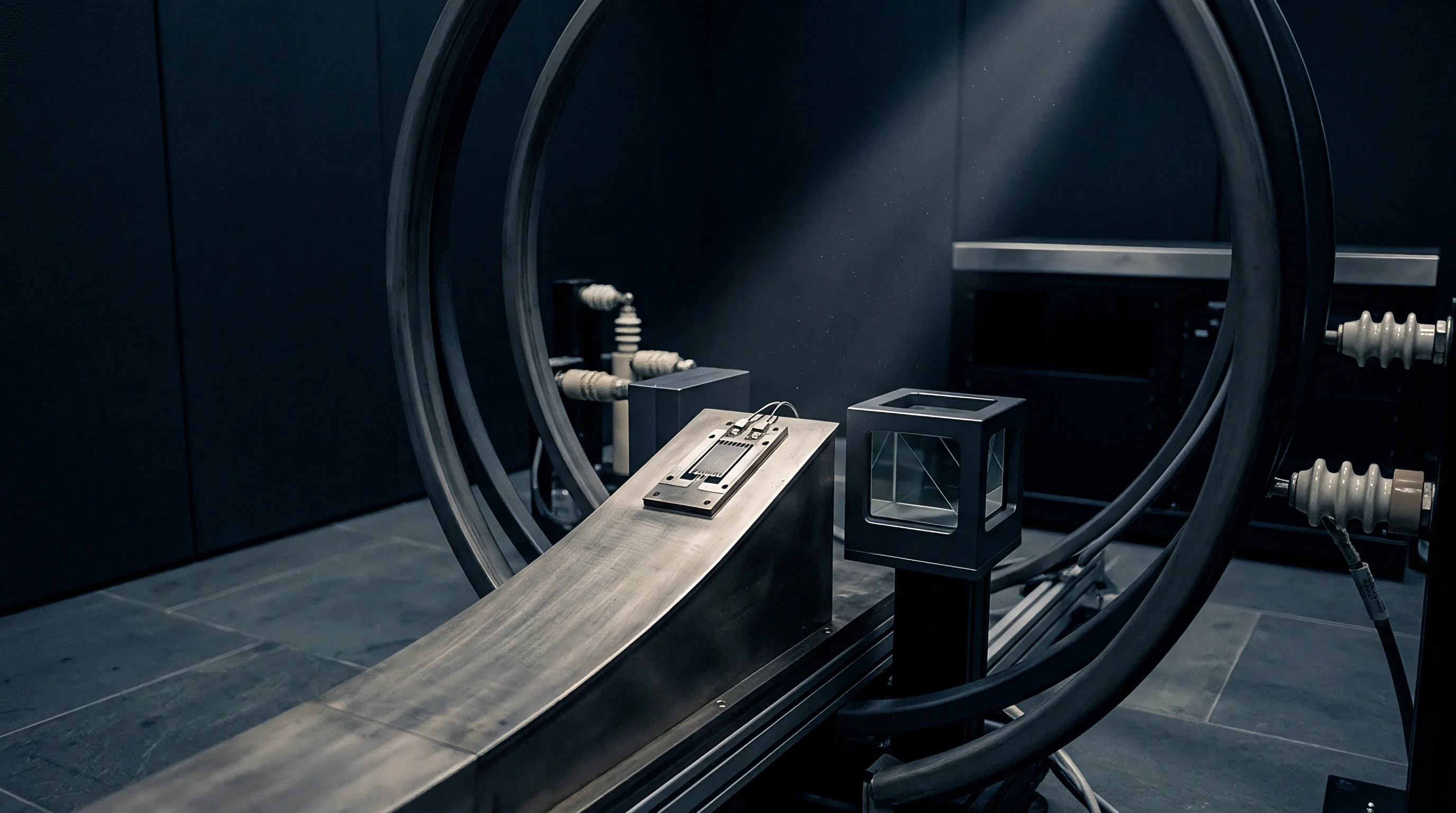
Separating gradient-induced errors from uniform temperature coefficients requires specialized test fixtures. Standard environmental chambers immerse the test assembly in circulating air, masking directional vulnerabilities. Measuring true gradient sensitivity requires applying controlled directional heat flux into specific package surfaces while monitoring the differential output.
Opposed Peltier modules clamped to a machined aluminum fixture provide direct gradient control. Driving one module to heat while the opposing unit cools allows varying the lateral gradient nabla T across the package while holding the mean body temperature steady. Fine-gauge micro-thermocouples bonded to package pins verify the boundary temperatures.
A structured sweep isolates mechanical strain from direct thermal transport effects:
- Mount the sensor enclosure onto a thermally isolated ceramic test fixture inside a shielded temperature test cell.
- Connect non-inductive low-noise excitation cabling between the sensor pins and an external baseline data acquisition system.
- Stabilize the ambient cell temperature at 25 degrees Celsius until all zero-offset readings settle within a 10-attofarad noise band.
- Apply a differential thermal step of 2.0 Kelvin across the dual Peltier actuators at a ramp rate of 0.5 Kelvin per second.
- Record the transient differential capacitance offset voltage continuously over a 300-second stabilization window.
- Reverse the Peltier drive polarities to apply an inverted gradient of identical magnitude to verify structural directional symmetry.
- Extract the spatial gradient drift coefficient expressed in femtofarads per Kelvin-per-millimeter from the steady-state baseline shift.
Mitigation Topologies and Dynamic Guarding
Mitigating gradient sensitivity at the layout level takes priority over firmware compensation. Active thermal guard rings embedded directly in the silicon die place micro-heaters and sensing diodes around the central capacitor cell. When the diodes register a lateral gradient, closed-loop driver circuits power the adjacent heaters to equalize temperatures across the perimeter of the active area.
| Mitigation Strategy | Gradient Reduction Ratio | Power Penalty (mW) | Board Area Impact | Implementation Stage |
|---|---|---|---|---|
| Symmetric High-Conductivity Copper Shunts | 3.5:1 | 0.0 | +15% PCB Area | Board Assembly |
| Silicon Interposer Active Guard Heaters | 12.0:1 | 18.5 | +5% Die Area | Silicon Fabrication |
| Dual-Die Cross-Coupled Capacitive Arrays | 8.0:1 | 0.0 | +100% Die Area | Silicon Design |
| Dual-Sensor Polynomial Firmware Mapping | 2.2:1 | 1.2 | 0% Hardware | Firmware Execution |
Peltier characterization demonstrates localized heating vulnerabilities, yet standard qualification tests run under uniform air streams, leaving directional conductive thermal management to system integration teams.


Supply

Sourcing Constraints and Datasheet Ambiguity
Selecting high-stability differential capacitive sensors involves navigating significant gaps in supplier datasheets. Manufacturers provide precision ratings, harmonic distortion specs, and uniform temperature coefficients in ppm per Kelvin, but almost never report gradient sensitivity figures or cross-die thermal time constants. System teams must therefore run their own characterization sweeps on incoming production lots.
Wafer processing determines fundamental gradient sensitivity. MEMS elements fabricated on silicon-on-insulator wafers with buried oxide layers establish very different heat paths than bulk silicon parts with conductive die-attach layers. Dual-die configurations that place matched sense elements side-by-side inside one package ease inventory sourcing, but the thermal barrier between dies leaves them vulnerable to lateral heat flows.
Monolithic topologies integrate opposing differential sense cells onto a single, centered silicon substrate, equalizing internal conduction paths and lowering gradient drift. However, monolithic dies carry a price premium and depend on a small group of specialized MEMS foundries, creating single-source exposure when capacity tightens.
Component datasheets routinely specify uniform thermal drift while omitting spatial thermal gradient parameters, shifting the burden of dynamic thermal qualification onto the buyer.
Procurement Verification Checklist
Evaluating parts for gradient-sensitive applications requires vetting qualification routines and process controls well beyond standard chamber cycling.
- Monolithic Die Construction verifies that differential sensing structures reside on a single silicon substrate rather than discrete bonded dies.
- Symmetrical Package Pinout confirms that power, ground, and signal lines route symmetrically to prevent uneven heat injection from board traces.
- AEC Q103 Thermal Shock Data confirms offset stability and mechanical integrity under rapid directional thermal ramping.
- Die Attach Voiding Limits established through scanning acoustic microscopy set maximum permissible voiding beneath sensing elements to preserve uniform thermal contact.
- Multi Point Temperature Sensing Integration confirms that onboard ASIC circuits monitor multiple internal temperature nodes to capture lateral gradients.
Supply agreements should stipulate maximum zero-g offset drift under specified lateral thermal ramp rates, establishing concrete criteria for batch rejection if incoming inspection reveals excessive gradient sensitivity.