Cross-Axis Substrate Thermal Diffusion Errors in Hermetically Sealed Micro-Machined Accelerometer Wafer Packages
Cross-axis thermal diffusion in sealed MEMS packages creates transient offset errors that evade static calibration and require symmetrical anchor layouts.

Gradient

Substrate Heat Transport
Lateral thermal conduction across single-crystal silicon substrates is fast, driven by the material’s high thermal conductivity of 148 W/m·K at 300 K. When an external heat pulse hits one edge of a hermetically sealed wafer-level package, energy spreads laterally across the die plane before vertical equilibrium is reached through the lid and cavity gas. Micro-machined accelerometer structures mounted directly above these die beds encounter localized temperature differences across their anchors while this heat propagates. Even a gradient of 0.05 °C across a 1.5 mm capacitive proof mass frame distorts internal stress fields unevenly, causing structural warping before the system can reach isothermal balance.
Hermetic capping introduces sharp thermal impedance drops across the wafer stack. Silicon cap wafers bonded with eutectic gold-tin seal rings carry thermal energy quickly around the perimeter while leaving the cavity gas ~ typically argon or nitrogen at low pressure ~ insulated inside. By comparison, borosilicate glass frit interfaces have a thermal conductivity near 1.1 W/m·K, functioning as a perimeter thermal barrier.
Heat entering through leadframe traces or solder bumps moves preferentially through high-density copper vias or metallic die-attach pads, setting up directional conduction paths across the active sensor plane.
Heat transfer across a multi-layer micro-machined stack follows three-dimensional pathways set by layer thickness, material interfaces, and cross-sectional area. The table below lists the thermomechanical properties that govern lateral energy diffusion in sealed wafer packages.
| Material / Layer | Thermal Conductivity (W/m·K) | Coefficient of Thermal Expansion (ppm/K) | Elastic Modulus (GPa) | Diffusivity (10⁻⁶ m²/s) |
|---|---|---|---|---|
| Single-Crystal Silicon (100) | 148.0 | 2.6 | 130.0 | 86.2 |
| Borosilicate Glass Cap | 1.1 | 3.25 | 64.0 | 0.62 |
| Gold-Tin (Au80Sn20) Eutectic Seal | 57.0 | 16.0 | 59.0 | 24.8 |
| Glass Frit Seal Interface | 1.0 | 6.8 | 40.0 | 0.45 |
| SAC305 Lead-Free Solder Bump | 58.0 | 22.0 | 51.0 | 31.5 |
Transient thermal gradients cause differential expansion between the upper cap wafer and the base substrate. Because the cap and base are tied together at the hermetic perimeter seal ring, this asymmetric expansion creates localized bending moments across the central cavity. Micro-machined suspension springs attached to internal anchors then experience asymmetric mechanical pre-loads as the cavity floor flexes.

Transient Cross-Axis Thermal Energy
Cross-axis sensitivity in a triaxial MEMS accelerometer die measures how much acceleration along one axis leaks into an orthogonal channel’s reading. Transient heat flux across the substrate disrupts this axis isolation. When a heat source ~ like an adjacent power management IC or an active high-power actuator channel ~ creates a lateral temperature difference, thermal expansion waves travel across the X-axis of the chip faster than vertical dissipation paths can move heat out along the Z-axis.
Standard qualification protocols under ISO 26262 require cross-axis isolation margins to remain intact under operational temperature ramps exceeding 10 °C per minute.
Substrate flexure from transient conduction displaces the structural anchors unevenly. A shift of just 0.2 nanometers at the anchor base of a high-aspect-ratio silicon comb finger array alters the baseline capacitive gap between fixed and movable fingers. When heat flows laterally along the X-axis, the frame rotates asymmetrically, producing a false acceleration signal on the Y- and Z-axis channels without any physical motion.
Thermal diffusion time constants scale with the square of the die’s characteristic length and inversely with thermal diffusivity. For a standard 2 mm by 2 mm silicon die with an effective thermal diffusivity of 86.2 × 10⁻⁶ m²/s, the diffusion time constant across the substrate plane is about 46 milliseconds. During this transient window, signal conditioning algorithms that rely on external static temperature sensors cannot track or correct internal mechanical distortion, leaving the system exposed to transient bias shifts.
Engineers must evaluate whether localized thermal gradients can be mapped dynamically using multi-point micro-thermocouple arrays embedded directly in the sensor package floor.


Strain

Asymmetric Frame Deflection
Deforming the silicon die bed disrupts the structural symmetry needed for high cross-axis rejection. In differential capacitive accelerometers, symmetrical springs cancel common-mode noise and uniform thermal expansion. But when lateral heat diffusion breaks this symmetry, spring stiffness on the warmer side drops relative to the cooler side.
Young’s modulus for single-crystal silicon decreases by roughly -60 ppm/°C; a 1 °C local thermal delta between opposing spring mounts shifts relative stiffness by 0.006 percent, producing measurable zero-g offset drift.
Suspensions designed for out-of-plane Z-axis detection use torsional flexures or asymmetric teeter-totter proof masses. Lateral thermal diffusion causes uneven expansion along the flexure hinge line, tilting the proof mass frame relative to the fixed electrode substrate. The resulting capacitive delta mimics a true Z-axis acceleration, even though it stems entirely from an X- or Y-axis thermal gradient.
The list below details key thermomechanical failure modes observed in hermetically sealed MEMS accelerometer packages subjected to directional heat pulses.
- Anchor Displacement Asymmetry occurs when localized heating expands one die anchor faster than adjacent mounts, causing rotation of the suspended sensor frame.
- Torsional Flexure Warpage arises from unequal thermal expansion across thin silicon flexure hinges, forcing out-of-plane proof mass tilting under purely planar heat flux.
- Cap-Substrate Bending Shear develops when CTE mismatch between cap glass and silicon base induces perimeter bending moments that flex the cavity floor.
- Comb Finger Pitch Distortion happens when transient lateral thermal diffusion varies stationary finger spacing across differential sense arrays, generating baseline offset errors.
Proof Mass Anchor Displacements
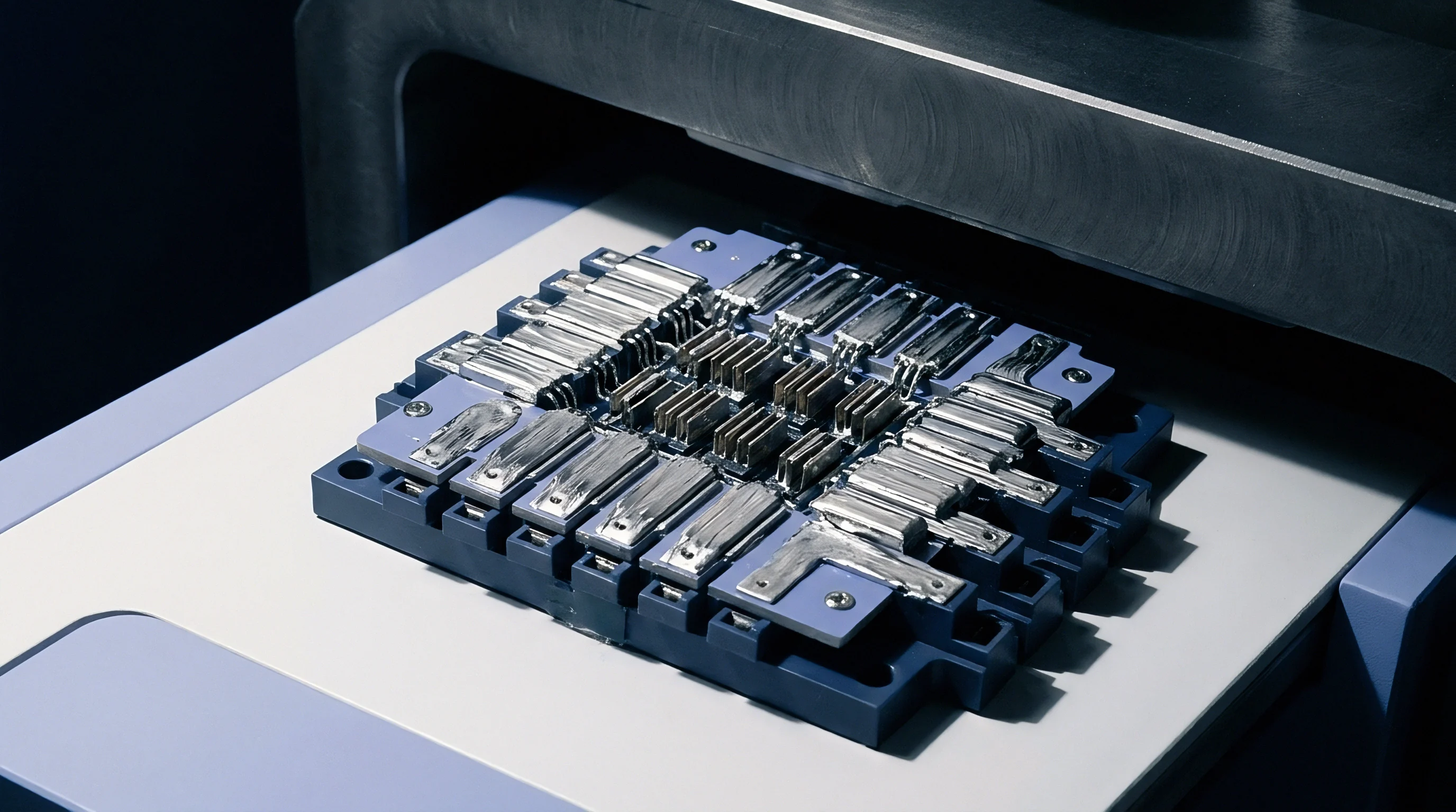
Mechanical anchors tie the MEMS frame to the underlying silicon substrate. Single-anchor designs centralize support to decouple the sensing element from die-attach stress, but remain sensitive to tilt-induced rotational moments. Multi-anchor layouts distribute loads effectively, but create closed kinematic loops vulnerable to substrate thermal strain.
Thermal diffusion between two anchors 1 mm apart creates a differential displacement delta delta-L equal to alpha times L times delta-T. Given a thermal expansion coefficient alpha of 2.6 ppm/K and a local gradient delta-T of 0.2 °C, anchor pitch stretches by 0.52 picometers, shifting differential capacitive balance.
Die-attach material properties govern how directly substrate strain passes into active sensing structures. Hard materials like gold-silicon eutectic preforms transfer package stress straight into the die bed. Soft organic adhesives ~ such as conductive silicone or flexible epoxy ~ dampen low-frequency stress, but introduce outgassing risk and absorb moisture over extended thermal cycling.
The table below outlines how common substrate bonding choices alter stress transmission into sealed cavities.
| Bonding Material Type | Glass Transition Temp (°C) | Storage Modulus below Tg (GPa) | Thermal Stress Coupling Index | Outgassing Potential (CVCM %) |
|---|---|---|---|---|
| Gold-Silicon (Au-Si) Eutectic | N/A (Melts 363 °C) | 83.0 | 0.95 | 0.00 |
| Silver-Filled Epoxy (High Elasticity) | 120.0 | 8.5 | 0.42 | 0.03 |
| Conductive Silicone Adhesive | -50.0 | 0.05 | 0.08 | 0.01 |
| Sintered Nano-Silver Paste | N/A (Sintered 260 °C) | 40.0 | 0.78 | 0.00 |
Asymmetric stress in the substrate triggers stress-birefringence and piezoresistive shifts. In doped silicon springs, these piezoresistive shifts change local electrical resistivity under thermal strain. While piezoresistive shifts do not change capacitive readings directly, they alter parasitic substrate resistance, degrading the signal-to-noise ratio in front-end charge amplifiers switching at high frequencies.
Centralized single-anchor topologies eliminate closed-loop mechanical thermal strain paths at the expense of higher out-of-plane mechanical shock susceptibility.

Asymmetry

Differential Capacitance Imbalance
Readout circuits in high-precision MEMS accelerometers detect sub-femtofarad capacitance shifts. Tactical-grade capacitive cells typically exhibit open-loop sensitivities of 10 to 50 fF/g, with baseline values around 1 pF per axis. When lateral thermal diffusion shifts fixed comb fingers by just 0.1 nanometers relative to movable fingers, the change delta-C equals baseline capacitance C-zero times the ratio of displacement to gap distance.
Across a 1.2 micrometer nominal gap, that tiny displacement produces an 83 fF shift ~ equivalent to a zero-g bias error over 1.6 g on a 50 g sensor.
Differential designs mitigate uniform thermal expansion by subtracting output set B from set A, where output voltage V-out equals supply voltage V-dd times (C1 – C2) / (C1 + C2). Uniform heating expands C1 and C2 equally, keeping (C1 – C2) near zero. Lateral thermal diffusion, however, subjects C1 to temperature T1 and C2 to T2.
This thermal difference breaks symmetry, pulling (C1 – C2) away from zero even without applied acceleration.
Integrated ASICs inside the cavity measure package temperature via an on-chip diode or PTAT cell. But sitting hundreds of micrometers from the proof mass center, the sensor reads ASIC die temperature rather than the mechanical frame’s thermal gradient. Standard factory calibration based on this remote diode cannot correct transient differential thermal bias errors.
Thermal calibration routines based on static equilibrium temperatures leave transient substrate gradient errors uncompensated.

Error Budget Allocation
Thermal diffusion errors account for a significant share of the total error budget in tactical-grade inertial measurement units. Systems often demand bias stability under 0.1 mg from -40 °C to +105 °C. Polynomial firmware models can trim static isothermal bias drift down to 0.02 mg/°C, but transient cross-axis thermal diffusion generates bias spikes up to 5 mg during rapid thermal changes ~ exceeding the noise floor by over two orders of magnitude.
Total zero-g bias error B-total under thermal load combines static isothermal drift, package stress hysteresis, and cross-axis diffusion errors, as detailed below.
| Error Component | Physical Root Cause | Magnitude (Typical) | Firmware Correctability | Primary Mitigation Path |
|---|---|---|---|---|
| Static Isothermal Bias Drift | Uniform CTE expansion and spring stiffness shift | 0.02 to 0.10 mg/°C | High (Polynomial Lookup) | Calibrated trim tables |
| Thermal Hysteresis | Die-attach relaxation and glass frit micro-plasticity | 0.20 to 1.50 mg | Low (History dependent) | Stress-isolating mounts |
| Cross-Axis Diffusion Bias Spike | Transient asymmetric substrate thermal expansion | 0.50 to 5.00 mg/(°C/s) | Very Low (Single sensor) | Symmetric layout and thermal shielding |
| Capacitive Parasitic Drift | Substrate dielectric permittivity temperature shift | 0.01 to 0.05 mg/°C | Moderate (On-chip ASIC reference) | Low-loss glass substrates |
Take a dual-axis accelerometer mounted on an industrial vehicle control board operating at 25 °C. An adjacent component dissipates power, causing a 2 °C/s thermal ramp along the package X-axis. With a cross-axis thermal diffusion bias coefficient of 1.2 mg/(°C/s), transient bias error reaches 2.4 mg within 1.5 seconds. If the safety system triggers at 1.0 mg, this uncompensated transient trips the system before the integrated thermal diode registers even a 0.5 °C rise.
Ignoring transient spatial thermal gradients in high-precision control loops results in unexpected system trips and degraded dead-reckoning navigation accuracy during thermal cycling.


Verification
Does Transient Diffusion Evade Standard Industrial Overtemperature Testing?
Standard qualification relies on thermal soak chambers where air temperature changes slowly ~ typically 1 °C to 2 °C per minute ~ while parts rest on heavy aluminum burn-in boards. These slow ramps allow the package, cavity, cap, and ASIC to reach isothermal equilibrium at each test point. Data collected this way produces clean, repeatable temperature coefficient curves, but hides cross-axis thermal diffusion errors completely.
Exposing diffusion errors requires generating controlled, localized transient thermal gradients across specific package axes while holding mechanical conditions steady. Verification test benches use targeted laser pulses or micro-heaters attached directly to individual package quadrants. Firing an infrared laser pulse at the positive X-axis lead while sampling raw capacitive outputs isolates the cross-axis diffusion transient from background mechanical noise.

Chamber Bench Characterization
Quantifying thermal diffusion errors requires precise test sequencing to isolate mechanical vibration, electromagnetic interference, and thermal effects. The following verification procedure outlines the bench steps used to measure transient cross-axis thermal sensitivity.
- Mount the hermetically sealed MEMS package onto a high-mass, low-thermal-conductivity ceramic test fixture isolated from ambient air currents.
- Establish baseline signal output across all three acceleration axes inside a temperature-controlled isolation chamber held at a constant 25.0 °C +/- 0.1 °C.
- Apply a localized step-input heat pulse to one side of the package using a contact micro-heater block powered by a precision current source.
- Record raw capacitive output data and internal ASIC temperature diode readings at a sample rate of at least 1 kHz for 60 seconds following heat application.
- Compute the transient bias spike amplitude by subtracting baseline isothermal offset from the peak output value registered during the transient heat propagation phase.
- Repeat the localized thermal pulse along orthogonal package axes to map cross-axis sensitivity matrices across X, Y, and Z axes.
Step-heating test data exhibits characteristic exponential rise and decay curves governed by internal silicon diffusion constants. Peak bias occurs when the spatial gradient across the spring anchors reaches its maximum differential.
Bench testing under MIL-STD-883 Method 1012 reveals that transient cross-axis bias spikes peak within 200 milliseconds of lateral thermal impulse application.
High-speed infrared thermography cameras fitted with microscopic lenses track real-time surface thermal profiles on unencapsulated packages during heating. Imaging confirms that heat moves through single-crystal silicon die beds in structured parabolic wavefronts, inducing local mechanical strain long before the cap or backing reaches isothermal equilibrium.
Baseline offset spikes are often dismissed on the grounds that application environments rarely experience unilateral point-source thermal transients in practical field deployments.


Mitigation

Structural Anchor Placement
Die-level design changes are the first defense against thermal diffusion errors. Centralized single-anchor designs place all suspension flexures around a single post at the geometric center of the sensor frame. Because heat waves radiate outward symmetrically from the center, local thermal expansion acts equally on all springs, preserving symmetry and capacitive balance.
Single-anchor frames lower cross-axis thermal bias spikes by up to 18 dB relative to four-corner quad-anchor designs.
When multi-anchor layouts are needed to survive shock levels over 10,000 g, symmetrical anchor placement rules apply. Aligning anchors with the silicon lattice’s neutral mechanical axis cuts stress coupling. Symmetrical thermal dummy structures placed around the active frame absorb lateral heat flux, smoothing sharp spatial gradients into uniform thermal fronts across the comb finger arrays.

Wafer Packaging Isolation
At the packaging level, matching the thermal expansion of perimeter bond materials reduces package-induced bending. Gold-tin eutectic bonding offers high seal strength and hermeticity exceeding MIL-STD-883 helium leak rates of 1 × 10⁻⁸ atm·cm³/s, though its high elastic modulus transfers thermal strain readily. Glass frit interfaces provide lower stiffness and better thermal isolation, but introduce larger CTE mismatches relative to silicon, raising perimeter stress during temperature swings.
The table below summarizes key thermomechanical and hermetic performance characteristics for major wafer-level packaging seal technologies used in micro-machined accelerometer manufacturing.
| Hermetic Seal Technology | Seal Ring Width (μm) | Processing Temp (°C) | Helium Leak Rate (atm·cm³/s) | Transient Thermal Isolation Index |
|---|---|---|---|---|
| Au-Sn Eutectic Bonding | 50 to 100 | 280 to 320 | < 1 × 10⁻⁹ | Low |
| Glass Frit Fusing | 150 to 300 | 420 to 450 | < 5 × 10⁻⁸ | High |
| Al-Ge Eutectic Bonding | 30 to 75 | 420 to 450 | < 1 × 10⁻⁹ | Moderate |
| Direct Silicon-to-Silicon Fusion | 10 to 30 | 800 to 1000 | < 1 × 10⁻¹⁰ | Very Low |
| Anodic Silicon-Glass Bonding | 100 to 200 | 350 to 400 | < 1 × 10⁻⁸ | Moderate |
Etching isolation trenches directly into the perimeter silicon substrate disrupts lateral heat conduction. Deep reactive-ion etching (DRIE) creates air gaps filled with low-pressure cavity gas that act as thermal barriers around the anchor zone. These barriers steer heat around the sensitive anchor region, flattening transient gradients across the capacitive frame.
Procurement specifications for aerospace-grade inertial sensors must mandate compliance with AEC-Q103-002 thermal shock standards, enforcing zero yield drops after 1,000 thermal shock cycles between -55 °C and +125 °C.
System designers must select substrate materials carefully to balance thermal diffusion isolation and mechanical shock survivability across the operating range.
Sourcing

Datasheet Specification Gaps
Commercial sensor datasheets rarely list transient cross-axis thermal diffusion specs. Instead, manufacturers emphasize static metrics like Temperature Coefficient of Offset (TCO) and Temperature Coefficient of Sensitivity (TCS) measured under steady soak conditions. A part with a great TCO of +/- 0.1 mg/°C can still exhibit bias spikes over 3.0 mg when exposed to dynamic heat pulses.
Sourcing engineers relying solely on standard datasheets risk selecting parts that fail under operational thermal transients.
Thorough evaluation requires requesting internal qualification dossiers. Complete records include step-response thermal transient curves, cross-axis transfer functions, and thermomechanical FEA models. Suppliers reluctant to share test methodologies often rely on aggressive digital filtering in ASIC firmware to hide thermal spikes, introducing uncalculated phase lag into host control loops.
Component selection requires auditing supplier testing methodologies against operational field conditions. The checklist below outlines essential verification criteria for evaluating accelerometer thermal performance prior to volume sourcing commitment.
- Transient Thermal Test Protocols must define heat pulse energy, application axis, and sampling rates used during dynamic thermal bias evaluation.
- Internal Sensor Architecture Data must specify anchor topology, package seal composition, and whether internal substrate thermal trenches are present.
- Firmware Filtering Latency must quantify the phase lag introduced by integrated ASIC digital filters used to suppress transient bias spikes.
- Hermeticity Testing Certificates must confirm helium leak rates post thermal-shock cycling according to MIL-STD-883 Method 1014 conditions.

Supplier Qualification Protocol
Establishing robust supply channels for high-reliability MEMS accelerometers requires a structured qualification framework. Component procurement involves technical evaluation, foundry audit, and batch testing stages to ensure long-term thermal stability.
- Review supplier die layout documentation to confirm structural anchor symmetry and mechanical isolation ring design.
- Conduct independent bench testing on sample lots using localized laser-pulse thermal excitation across X, Y, and Z package axes.
- Audit foundry wafer-bonding processes to ensure seal-ring width and cavity vacuum levels meet hermeticity stability standards over production runs.
- Insert explicit transient thermal bias drift limits into the master component purchasing specification document.
- Mandate continuous burn-in screening with dynamic thermal cycling for every incoming production lot.
Second-sourcing tactical-grade accelerometers presents real difficulties. Parts from different foundries may share identical pinouts and footprints while using completely different anchor geometries or cap seal materials. Swapping a glass-frit dual-anchor sensor for an aluminum-germanium single-anchor alternative breaks host thermal compensation algorithms, requiring firmware rewrites and full re-qualification.
Wafer fabrication yields hinge on controlling stress along the perimeter bond. Micro-cracks in glass frit seal rings, caused by thermal mismatch during wafer bonding, form slow helium leak paths that degrade cavity vacuum over time. As cavity pressure rises from 1 mbar to 100 mbar, gas damping increases, altering frequency response and adding damping phase errors on top of thermal diffusion effects.
Total landed cost calculations for precision accelerometers must account for yield loss at screening, thermal calibration overhead, and field liability from uncompensated thermal transients. Selecting components designed with built-in thermal isolation reduces downstream software complexity and overall lifecycle costs.