High Temperature Thin Film Strain Sensor Calibration and Mounting
High temperature thin film strain sensor accuracy depends on rigorous apparent strain polynomial correction, dielectric barrier integrity, and drift mitigation.


Sputter
Physical vapor deposition forms the structural foundation of high-temperature thin-film strain sensors. Sputtering micro-scale sensing elements directly onto structural components eliminates the thick, creep-prone organic backings typical of foil gauges. Operating above eight hundred degrees Celsius requires a multi-layer thin-film stack where each material serves a distinct electrical, thermal, or mechanical role.
Base components in these environments are typically nickel-based superalloys like Inconel 718, René 41, or single-crystal CMSX-4, all of which exhibit high thermal expansion coefficients between thirteen and fifteen parts per million per degree Celsius. Because direct contact between a metallic sensing film and a conductive superalloy causes an immediate electrical short, laying down a dense, defect-free dielectric insulation layer is the critical first step in fabrication.
Multi-layer stacks are deposited in magnetron sputtering chambers at base pressures below five times ten to the minus seven Torr. Dielectric isolation layers are grown using radio-frequency magnetron sputtering, while direct-current magnetron sputtering handles the metallic piezoresistive sensing films. Insulation layers generally run between three and eight micrometers thick.
If the insulation is too thin, the film risks pinholes, substrate element diffusion, and high-temperature electrical breakdown; if too thick, accumulated mechanical strain energy triggers cracking, delamination, and spallation during rapid thermal swings. Mechanical stability at high temperatures depends on dialing in the deposition parameters, ambient gas pressure, substrate bias voltage, and subsequent annealing cycles.

Substrate Dielectric Insulation Architecture
Dielectric barriers separate sensing grids from conductive superalloy substrates. Alpha-phase aluminum oxide and yttria-stabilized zirconia are the standard choices here. Aluminum oxide offers high electrical resistivity ~ exceeding ten to the eighth ohm-centimeters at room temperature and holding above ten to the fifth ohm-centimeters at one thousand degrees Celsius.
However, depositing pure aluminum oxide via RF sputtering frequently yields amorphous or mixed-phase films with high internal tensile stress. Sputtering an initial metallic aluminum or chromium bond coat of fifty to one hundred nanometers promotes adhesion to the superalloy before reactive sputtering in an argon-oxygen plasma forms the stoichiometric alumina film.
Thermal expansion mismatch between the ceramic insulation and the metal substrate generates severe shear stress during thermal cycling. Aluminum oxide has a coefficient of thermal expansion around eight parts per million per degree Celsius, whereas nickel-based superalloys expand at nearly twice that rate. Heating the assembly to one thousand degrees Celsius drives the alumina into heavy compression, which flips to tension upon cooling.
Using a functionally graded dielectric stack or a dual-layer architecture relieves much of this stress. Yttria-stabilized zirconia expands at roughly ten to eleven parts per million per degree Celsius, matching the superalloy much more closely. Placing a YSZ layer against the substrate and capping it with aluminum oxide mitigates expansion mismatch without sacrificing high-temperature electrical insulation.

Metallic and Ceramic Piezoresistive Film Alloys
Grid material selection is a compromise between thermal stability, temperature coefficient of resistance, and oxidation resistance. Standard nickel-chromium alloys degrade rapidly above six hundred degrees Celsius from phase transformations and rapid oxidation. High-temperature thin films turn instead to palladium-chromium, platinum-rhodium, or conductive ceramics such as indium tin oxide.
Palladium-chromium at an atomic ratio of eighty-seven percent palladium to thirteen percent chromium by weight is a common choice up to one thousand degrees Celsius. When heated in oxygen, it develops a self-healing surface scale of chromium oxide, leaving the underlying alloy matrix stable and phase-change-free for repeatable resistance-temperature behavior.
| Material Stack Layer | Nominal Composition | Deposition Method | CTE (ppm/°C) | Max Temp (°C) | Resistivity at 1000°C (µΩ·cm) |
|---|---|---|---|---|---|
| Dielectric Base Layer | Al2O3 (99.99%) | RF Magnetron Sputtering | 8.1 | 1100 | 10^11 |
| Graded Dielectric | 8YSZ (8 mol% Y2O3-ZrO2) | RF Magnetron Sputtering | 10.5 | 1250 | 10^8 |
| Piezoresistive Grid | Pd-13wt%Cr | DC Magnetron Sputtering | 13.5 | 1000 | 115 |
| High-Temp Piezoresistor | Pt-13wt%Rh | DC Magnetron Sputtering | 10.3 | 1400 | 42 |
| Ceramic Piezoresistor | ITO (90 In2O3 / 10 SnO2) | Reactive RF Sputtering | 8.5 | 1500 | 8500 |
Platinum-rhodium alloys, like platinum with thirteen percent rhodium, provide exceptional oxidation resistance beyond twelve hundred degrees Celsius. The tradeoff is a high temperature coefficient of resistance, generating large thermal output signals that demand extensive mathematical compensation. Indium tin oxide films offer a non-metallic option usable up to fifteen hundred degrees Celsius in oxidizing environments, with piezoresistive gauge factors between four and ten ~ well above the typical metallic value of two.
Ceramic films also have much higher baseline resistivity, enabling smaller gauge footprints with high nominal resistance. Depositing ceramic piezoresistors requires tight control of oxygen partial pressure during reactive sputtering to maintain stoichiometry and carrier concentration.
Failure modes in micro-fabricated thin-film stacks during extreme thermal cycling arise from physical and chemical degradation mechanisms acting simultaneously at interfaces:
- Dielectric Barrier Delamination High thermal expansion mismatch between the metal substrate and ceramic insulation causes adhesive fracture during cooling.
- Phase Transformation Stress Metallurgical phase changes within the piezoresistive grid introduce unpredictable resistance steps above 800°C.
- Interdiffusion Contamination Migration of substrate elements through thin dielectric films degrades electrical isolation at high temperatures.
- Substrate Oxidation Heave Oxygen penetration through porous thin films expands the metallic substrate surface, tearing the sensor grid.
Films are patterned into strain-sensing geometries via photolithography or shadow masking. Laser-cut molybdenum or stainless steel shadow masks aligned inside the vacuum chamber avoid the chemical contamination associated with photoresists and wet etchants. Photolithography, by contrast, resolves finer line widths down to five micrometers, enabling compact grids on curved blade surfaces.
Both methods produce a serpentine grid terminating in thick contact pads for micro-welding or high-temperature micro-brazing. Sputtering platinum or gold over these pad regions cuts contact resistance and guards against oxidation during lead attachment.
Thicker ceramic dielectric barriers reduce electrical leakage at elevated temperatures but increase mechanical shear stress within the strain-sensing film stack.
Post-deposition thermal annealing stabilizes the microstructure and relieves residual stress in sputtered films, which otherwise retain high lattice defect densities, trapped argon, and non-equilibrium crystal structures. Soaking the parts in a furnace at or just above their intended operating temperature drives recrystallization, grain growth, and stress relaxation. Annealing palladium-chromium sensors in air at eight hundred degrees Celsius for several hours establishes the protective chromium oxide scale, preventing drift during subsequent operational runs.
When resistance drift exceeds specification limits early in testing, target material purity and chamber gas contamination are typically the root causes.

Mount
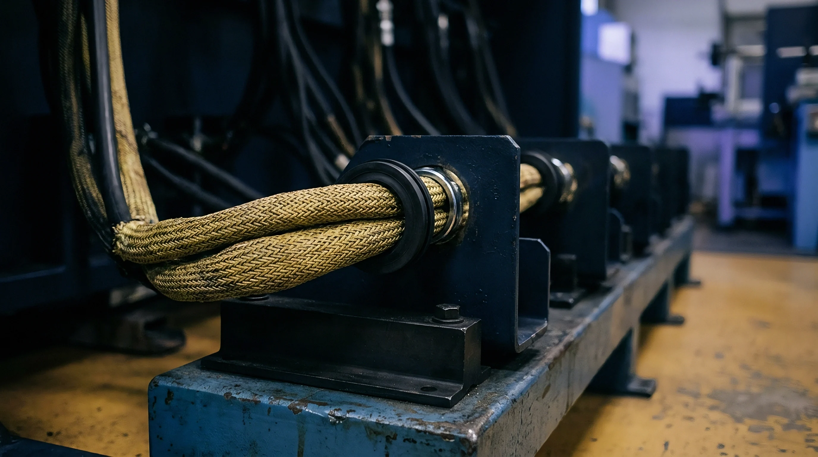
Mounting thin-film sensors on high-temperature turbomachinery requires careful management of thermal expansion stresses. Direct deposition remains the benchmark, forming an atomic bond between the dielectric layer and the structural component. Even so, placing full-scale gas turbine disks or large steam casing sections into high-vacuum sputtering chambers is often physically impossible.
Component dimensions, chamber geometry, and turnaround times frequently require indirect mounting instead. Here, thin-film sensors are prefabricated on metal foil shims and joined to host components via high-temperature ceramic cements, laser spot welding, or transient liquid phase bonding.
Foil backings are typically twenty-five to fifty micrometers thick, stamped from oxidation-resistant alloys like Inconel 600, Hastelloy X, or FeCrAl. These pre-sensorized foils undergo full sputtering, patterning, and preliminary heat treatment prior to installation in the field. Transferring strain from the host structure through the shim requires a bonding agent that withstands heavy vibration and sharp thermal gradients.
High-temperature ceramic cements handle these environments past eleven hundred degrees Celsius. Formulations rely on inorganic silicate, phosphate, or aluminosilicate binders blended with fine powders of alumina, zirconia, or silicon carbide.

Interfacial Shear and Strain Transfer Mechanics
Applied mechanical load travels from the host component into the piezoresistive grid through the ceramic layers. Directly deposited films transfer strain with near-total fidelity because of their sub-micron thickness and atomic interface bonds, routinely exceeding ninety-nine point nine percent strain transfer up to the substrate yield point. Foil sensors attached with ceramic cements are limited by the shear modulus and thickness of the adhesive layer.
As operating temperatures climb, inorganic binders soften, lowering the shear modulus and causing strain transfer losses where the measured strain at the gauge surface falls below that of the host component.
Surface curvature introduces significant peeling stress along the edges of foil gauges. Bending moments across the adhesive joint scale with adhesive thickness and foil stiffness, making thin, uniform adhesive applications between fifty and seventy-five micrometers essential. Heavier adhesive layers invite internal voids, micro-cracking, and non-uniform stress profiles.
Thermal expansion mismatches across the metal substrate, ceramic adhesive, and foil backing generate local residual stresses that destabilize zero points. Tailoring adhesive formulations to match the host material’s thermal expansion coefficient minimizes interfacial shear and extends fatigue life under thermal cycling.

High Temperature Ceramic Cement Attachment Procedures
When component size prevents direct deposition on turbine blades, ceramic cement attachment serves as the primary field alternative. Success hinges on surface prep, powder-to-liquid mixing ratios, and a disciplined curing cycle. The following sequence details the installation of foil-backed thin-film strain sensors using aluminosilicate adhesives:
- Clean the substrate surface using ultrasonic solvent baths and plasma etching to eliminate organic residues.
- Grit-blast the installation area with fifty-micrometer aluminum oxide media at forty pounds per square inch pressure to achieve a uniform surface roughness of two to three micrometers Ra.
- Apply a thin primer coat of inorganic ceramic binder to the grit-blasted substrate using a micro-spray gun, achieving a uniform thickness of ten micrometers.
- Position the pre-fabricated thin-film sensor foil onto the primed substrate using alignment fixtures under optical magnification.
- Dispense the fully mixed ceramic cement across the foil edges using a syringe dispenser, ensuring air bubble entrapment is eliminated.
- Clamp the assembly under a constant mechanical pressure of zero point two megapascals using spring-loaded high-temperature fixtures.
- Ramp the component furnace at two degrees Celsius per minute up to one hundred twenty degrees Celsius and hold for two hours to evaporate water carrier solvents.
- Escalate furnace temperature at three degrees Celsius per minute to four hundred degrees Celsius for two hours to convert chemical binders into crystalline ceramic structures.
- Perform a final thermal soak at eight hundred degrees Celsius for four hours to achieve full mechanical density and relieve residual processing stresses.
Leadwire attachment is another frequent point of mechanical and electrical failure. Sensor grids need low-resistance terminations that survive severe centrifugal loads and aerodynamic turbulence. Standard leadwire stock consists of round or ribbon-shaped platinum or platinum-rhodium wire between seventy-five and one hundred fifty micrometers in diameter.
Micro-resistance spot welding or parallel-gap laser welding joins these wires directly to the sputtered contact pads. Laser welding provides tight energy control, fusing the wire to the pad without puncturing the underlying dielectric insulation.
Dynamic vibration inside turbomachinery readily fatigues leadwires at the weld joint. Relieving this stress requires anchoring the leads within five millimeters of the pads using ceramic cement straps, ceramic sleeving, or spot-welded foil tabs. Leads are then routed through insulated ceramic tubing toward telemetry or slip-ring hardware.
Cutting corners on surface prep or cement curing schedules risks total debonding during thermal shock, turning an expensive turbine test into scrap.

Rig
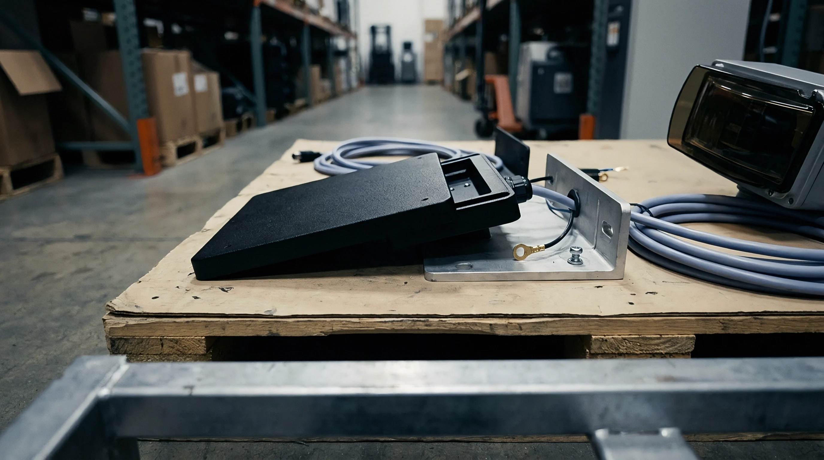
Validating thin-film strain gauges at eleven hundred degrees Celsius requires tight control over mechanical load, thermal profiles, and instrumentation. Ambient calibration hardware cannot handle these temperatures or maintain spatial temperature uniformity. High-temperature test setups integrate multi-zone tube furnaces, precision actuators, optical metrology, and high-impedance data acquisition systems.
These rigs evaluate gauge factor shift with temperature, apparent strain profiles, linearity, hysteresis, and long-term zero drift under thermal soak.
Thermal gradients across the test specimen degrade measurement accuracy. Calibration rigs use three-zone or five-zone tube furnaces governed by independent PID controllers. Thermocouples arrayed along the calibration beam track temperature distributions to keep gradients within plus or minus zero point five degrees Celsius across the gauge area.
When evaluating materials prone to rapid oxidation or microstructural breakdown, the beam must be housed in a vacuum chamber or inert gas enclosure.

Four Point Bending Quartz Tube Furnace Rigs
Applying uniform strain across a hot-zone specimen demands purpose-built fixtures. Four-point bending rigs generate a central span of constant bending moment where transverse shear forces drop to zero. Test beams are machined from high-temperature superalloys, silicon nitride ceramics, or single-crystal sapphire.
Sapphire maintains linear elasticity and mechanical strength up to fifteen hundred degrees Celsius, preventing plastic deformation of the beam during loading cycles.
| Rig Component | Operating Temperature Range | Loading / Measurement Method | Measurement Resolution | Environmental Atmosphere |
|---|---|---|---|---|
| Four-Point Bending Fixture | 20°C to 1200°C | Pneumatic / Servo-Hydraulic | ±0.1 N Force | Air, Vacuum, High-Purity Argon |
| Cantilever Thermal Load Rig | 20°C to 800°C | Precision Dead Weight / Screw Drive | ±0.5 µm Displacement | Ambient Air |
| 3D Optical Extensometer | 20°C to 1500°C | Dual-Camera Digital Image Correlation | ±5 Microstrain | Quartz Window Viewport |
| Laser Interferometric Extensometer | 20°C to 1400°C | Heterodyne Doppler Interferometry | ±0.1 Microstrain | Controlled Inert Environment |
Loading rods made from high-purity fused quartz or sintered silicon carbide enter the furnace through dynamic vacuum seals, actuated externally by screw-driven test frames or pneumatic cylinders. Placing load cells outside the hot zone isolates force measurements from thermal drift. Theoretical surface strain is calculated directly from measured load and beam geometry.
Pin friction, knife-edge wear, and thermal expansion of the loading train must be characterized and subtracted from the raw data.

Optical Extensometry and Laser Interferometric Metrology
Contact extensometers introduce thermal conduction paths and localized mechanical loading inside high-temperature zones. Ceramic contact rods can also scuff delicate thin-film grids or distort local heat transfer. Optical strain metrology avoids these issues entirely by measuring surface displacement through transparent quartz viewports without physical contact.
3D Digital Image Correlation systems track high-contrast speckle patterns applied to the beam adjacent to the sensor. Speckle patterns rely on ceramic paints, powder dusting, or laser-etched microtextures capable of withstanding fifteen hundred degrees Celsius without spalling. Dual digital cameras image the pattern through the viewport during mechanical loading.
Optical bandpass filtering combined with monochromatic laser illumination cuts through specimen incandescence above eight hundred degrees Celsius, ensuring clean tracking.
Laser heterodyne interferometry offers sub-microstrain resolution by directing beams at ceramic targets or micro-notches on the beam surface. The reflected signals yield direct displacement data. The high-temperature gauge factor is extracted by correlating this optically measured surface strain against the electrical resistance change of the sensor.
Specification of ASTM E251 compliance for high-temperature strain measurements obligates suppliers to verify gauge factor variation up to the maximum operating temperature limit.
Traceable measurement requires adherence to standardized testing methods. Metrologists adapt ASTM E251, originally developed for bonded metallic resistance gauges, to thin-film sensors. Invoking ASTM E251 clause 7.3 places the burden of thermal soak stability on the testing laboratory, requiring full documentation of furnace gradient limits.


Output
Exposing thin-film gauges to high temperatures causes resistance shifts unrelated to mechanical strain. This apparent strain is a central challenge in high-temperature metrology, arising from the alloy’s intrinsic temperature coefficient of resistance and the thermal expansion mismatch between the grid and substrate. Uncorrected thermal output often exceeds real mechanical strain signals by an order of magnitude during turbine testing.
The total fractional change in electrical resistance of an uncompensated thin-film strain sensor subjected to both thermal and mechanical excitation follows a strict mathematical relationship:
The total fractional resistance change equals the product of the gauge factor and mechanical strain, plus the combined temperature coefficient of resistance and differential thermal expansion term multiplied by temperature change. Mathematically, this is expressed as: ΔR / R_0 = (S_g × ε_mech) + × ΔT. Here, S_g represents the gauge factor, ε_mech represents true mechanical strain, α_TCR represents the temperature coefficient of resistance of the film alloy, α_sub represents the coefficient of thermal expansion of the substrate, α_grid represents the thermal expansion coefficient of the piezoresistive grid, and ΔT represents temperature change relative to a reference baseline.
Palladium-chromium film grids at 900°C exhibit a zero shift of 42 microstrain after fifty hours of thermal soak. Evaluating thin-film strain gauge installations on nickel-based superalloys requires calculating the differential thermal expansion across the dielectric barrier. Thermal output curves from room temperature up to 1050°C are tracked using fourth-order polynomial fitting algorithms, while quantifying gauge factor shifts across thermal cycles relies on referencing high-precision optical extensometer displacements.

Thermal Polynomial Extraction and Apparent Correction
Separating mechanical strain from thermal output across varying operating temperatures requires mathematical correction. Before operational runs, sensorized components undergo unloaded calibration sweeps in an isothermal furnace. Heating and cooling rates must mimic field profiles to capture thermal hysteresis, with the resulting zero-load resistance records defining the raw apparent strain profile.
Third- or fourth-order polynomials fitted to this temperature-versus-apparent-strain data provide the compensation curves used in data post-processing. A standard fourth-order model takes the form:
Apparent strain ε_app(T) = A_0 + A_1 × T + A_2 × T^2 + A_3 × T^3 + A_4 × T^4, where T represents measured temperature in degrees Celsius, and A_0 through A_4 represent empirical regression coefficients. In test runs, adjacent thermocouples log local temperatures, allowing software to calculate instantaneous apparent strain and subtract it from total measured strain to isolate the mechanical signal.
What Compensates Oxidation Kinetic Resistance Shift above Eight Hundred Degrees?
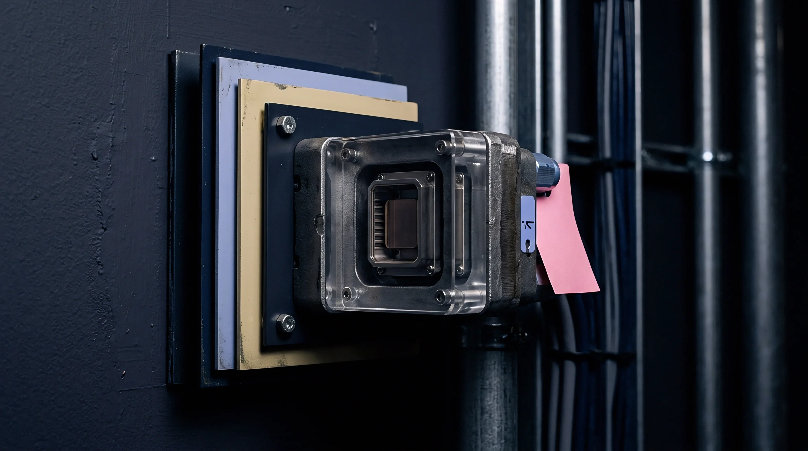
Extended high-temperature exposure promotes oxygen diffusion into metallic grids, reducing their effective cross-sectional area. Short calibration sweeps do not capture this time-dependent drift. Palladium-chromium exposed to air at nine hundred degrees Celsius undergoes selective chromium oxidation to build its protective scale, drawing chromium from the bulk alloy and shifting the remaining matrix toward pure palladium.
Because the temperature coefficient of resistance in Pd-Cr depends on exact chromium content, this depletion causes steady baseline drift and alters the gauge factor over time.
Lattice recovery, stress relaxation, and grain boundary diffusion also drive zero drift. Sputtered films are deposited in non-equilibrium states; holding them at high temperatures accelerates grain growth and eliminates defects, permanently altering resistivity. If uncompensated, oxidation-induced resistance growth registers as false mechanical strain during steady-state thermal soaks.
Dual-element self-compensating patterns help mitigate both apparent strain and baseline drift. These gauges place two identical grids side by side on the dielectric layer. One grid aligns with the principal stress axis to measure mechanical strain plus thermal output, while the second sits perpendicular to the strain field or on an adjacent decoupled tab, experiencing the same thermal environment but no mechanical load.
Wiring them into adjacent arms of a Wheatstone bridge cancels common-mode thermal output and drift in real time.
For bridge compensation to work, both elements must share identical resistance, temperature coefficients, and oxidation rates over time. Temperature gradients across the pair break bridge symmetry, leaving residual uncompensated error. Modern data systems typically combine bridge compensation with polynomial post-processing to maximize accuracy in turbomachinery testing.
Isolating grain boundary oxidation drift from genuine mechanical strain during multi-day runs past one thousand degrees Celsius remains an ongoing challenge.


Budget
Determining total measurement uncertainty for high-temperature strain testing requires tracking variance across thermal, mechanical, and electrical subsystems. Metrology in these environments involves coupled error sources that behave non-linearly. Applying room-temperature tolerances yields overly optimistic bounds.
Realistic uncertainty budgets follow the ISO/IEC Guide to the Expression of Uncertainty in Measurement, combining Type A statistical data with Type B systematic evaluations.
Gauge factor sensitivity to temperature is a primary driver of measurement uncertainty. The gauge factor of palladium-chromium thin films drops roughly zero point zero two percent per degree Celsius. Testing at one thousand degrees Celsius without correcting for this shift causes a systematic strain underestimation of nearly twenty percent.
Other major contributors include thermocouple tolerances, bridge non-linearity, leadwire resistance drift, signal conditioning noise, and residual polynomial fitting errors.

Component Uncertainty Contributions in High Temperature Measurements
Systematic and random errors are combined into an expanded uncertainty value via root-sum-square calculation. Each standard uncertainty u_i reflects a one-sigma bound, scaled by a sensitivity coefficient c_i that defines its impact on final strain output. Combined standard uncertainty u_c is computed by summing the squared products across all identified physical error sources.
| Uncertainty Component Source | Probability Distribution Type | Standard Uncertainty Value | Sensitivity Coefficient | Uncertainty Contribution (µε) | |
|---|---|---|---|---|---|
| Apparent Strain Polynomial Residual | Normal (Type A) | ±15.0 µε | 1.0 | 15.0 | |
| Thermocouple Temperature Error | Normal (Type B) | ±1.5 °C | 2.8 µε/°C | 4.2 | |
| Gauge Factor Temperature Correction | Rectangular (Type B) | ±1.2 % | 1000 µε / 100% | 12.0 | |
| Leadwire Resistance Thermal Drift | Rectangular (Type B) | ±0.08 Ω | 8.5 µε/Ω | 0.68 | |
| Dielectric Leakage Resistance Drop | Normal (Type B) | ±0.5 MΩ | 5.2 µε/MΩ | 2.6 | |
| Instrumentation ADC Non-Linearity | Rectangular (Type B) | ±0.005 % FS | 2000 µε / 100% | 0.10 | |
| Combined Standard Uncertainty (u_c): ±19.8 Microstrain | Expanded Uncertainty (K=2, 95% Confidence): ±39.6 Microstrain | |||||
Uncertainty widens sharply as temperatures rise. Dielectric breakdown across thin ceramic barriers introduces severe bias at elevated temperatures. By one thousand degrees Celsius, the insulation resistance of sputtered alumina falls from giga-ohms to fractional mega-ohms.
This creates a parallel leakage path across the grid that shunts excitation current away from the sensor, suppressing recorded signal amplitudes. Lead shielding and yttria-stabilized zirconia barrier layers help control these shunting errors.
Traceability Chain and Calibration Interval Planning
Documenting traceable calibration to national metrology institutes is essential for critical turbine evaluations. Primary standards for strain calibration rely on optical displacement metrology traceable to national physical laboratories. Reference thermocouples used during thermal sweeps require periodic calibration against fixed-point standards like the freezing points of gold or silver.
Recalibration schedules for thin-film sensors differ fundamentally from those of reusable load cells. Direct-deposited gauges cannot be removed from structural hardware for bench recalibration without destroying the sensor. Quality assurance programs rely instead on field verification with co-located sensors, periodic optical checks, or zero-load thermal sweeps during scheduled engine shutdowns.
An accredited high-temperature calibration record includes:
- Traceable Temperature Records Documented thermal profiles from calibrated thermocouples positioned within ten millimeters of the sensor grid during testing.
- Apparent Strain Polynomial Coefficients Third or fourth-order mathematical descriptions of resistance change versus temperature under zero mechanical load conditions.
- Gauge Factor Temperature Coefficients Measured sensitivity variations expressed as percentage changes per hundred degrees Celsius relative to room temperature baselines.
- Uncertainty Budget Breakdowns Itemized listings of combined standard uncertainties with declared coverage factors and confidence intervals.
Calibration certificates for high-temperature sensors must state combined uncertainty and explicit coverage factors, typically using K equals two for a ninety-five percent confidence interval. Omitting temperature-dependent gauge factor shifts or dielectric leakage paths severely underestimates operational error. Narrow temperature sweeps during sensor qualification often hide large measurement errors that surface when components encounter unmodeled transient thermal loads.


Allowance
Procuring high-temperature thin-film sensors involves balancing cleanroom fabrication yields, specialized manufacturing steps, and strict validation criteria. Buyers pay primarily for verified metrology rather than raw hardware. Unlike foil gauges produced on continuous roll lines, thin-film gauges are cleanroom devices vulnerable to fabrication fallout.
Shadow mask tooling, target material certifications, vacuum chamber run time, and post-deposition heat treatments all contribute to total acquisition cost.
Procurement specs that lack explicit environmental envelopes lead to rejected lots and budget overruns. Specifying a resistance tolerance without defining operating temperature, allowable drift rates, and substrate alloy composition forces vendors to price in large safety margins. Complete procurement planning must account for cleanroom sputtering, lead termination, individual thermal sweeps, and field installation services.
Commercial Tolerance Pricing and Yield Factors
Demanding tight tolerances on initial resistance and gauge factor drives unit costs up quickly. Film thickness varies across chamber platens, typically yielding as-sputtered resistance spreads of plus or minus ten percent within a single batch. Constraining nominal resistance to plus or minus one percent requires laser trimming individual grids.
The following comparison illustrates pricing tiers for palladium-chromium thin-film strain gauges:
| Sensor Specification Grade | Nominal Resistance Tolerance | Max Temp Rating (°C) | Included Calibration Dossier Data | Estimated Unit Price (USD) |
|---|---|---|---|---|
| Industrial Evaluation Grade | ±10 % | 700 | Room Temp Gauge Factor Only | $450 – $650 |
| Aerospace Test Standard | ±5 % | 900 | Full Apparent Strain Polynomial Fit | $1,200 – $1,800 |
| Precision Metrology Grade | ±1 % (Laser Trimmed) | 1050 | Full Thermal Sweep, GF vs Temp, Traceable Uncertainty Budget | $3,200 – $5,500 |
| Nuclear / Space Flight Qualified | ±0.5 % | 1200 | Multi-Cycle Drift Verification, Destructive Witness Coupon Report | $8,500 – $14,000 |
Operating temperature requirements drive cleanroom costs. Sensors rated above one thousand degrees Celsius demand high-purity ceramic targets, multi-layer dielectric stress balancing, platinum lead laser welding, and multi-day pre-oxidation annealing. For complex multi-layer ITO ceramic gauges operating at fifteen hundred degrees Celsius, batch yield losses can exceed fifty percent.

Contractual Acceptance Clauses and Field Recalibration Expenses
Procurement contracts must clearly establish acceptance criteria for thermal stability, insulation resistance, and room-temperature gauge factor. Standard agreements include receiving inspections with baseline resistance checks and dielectric testing at five hundred volts DC. Room-temperature insulation resistance below one hundred mega-ohms points to pinhole defects or ceramic contamination, warranting lot rejection.
High-temperature acceptance protocols require well-defined verification steps. Contracts often mandate witness coupons processed alongside flight hardware, allowing destructive testing of adhesion, SEM thickness verification, and grain structure analysis without harming test components. Requiring certified apparent strain polynomial fits for every delivered gauge transfers calibration overhead to the vendor before delivery.
Field maintenance budgets must cover scheduled thermal sweeps, optical verification runs, and sensor replacement cycles. Turbine test programs allocate substantial time to pre-test calibration checks. Over multi-year campaigns, purchasing pre-conditioned and fully characterized sensor lots proves more cost-effective, as longer thermal exposure steadily widens uncertainty bounds on unconditioned gauges.