Thermal Soak Chamber Baseline Configuration for MEMS Accelerometer Testing
MEMS accelerometer thermal soak testing demands controlled airflow, CTE-matched carrier substrates, low-EMF cabling, and verified steady-state dwell times.
Plenum
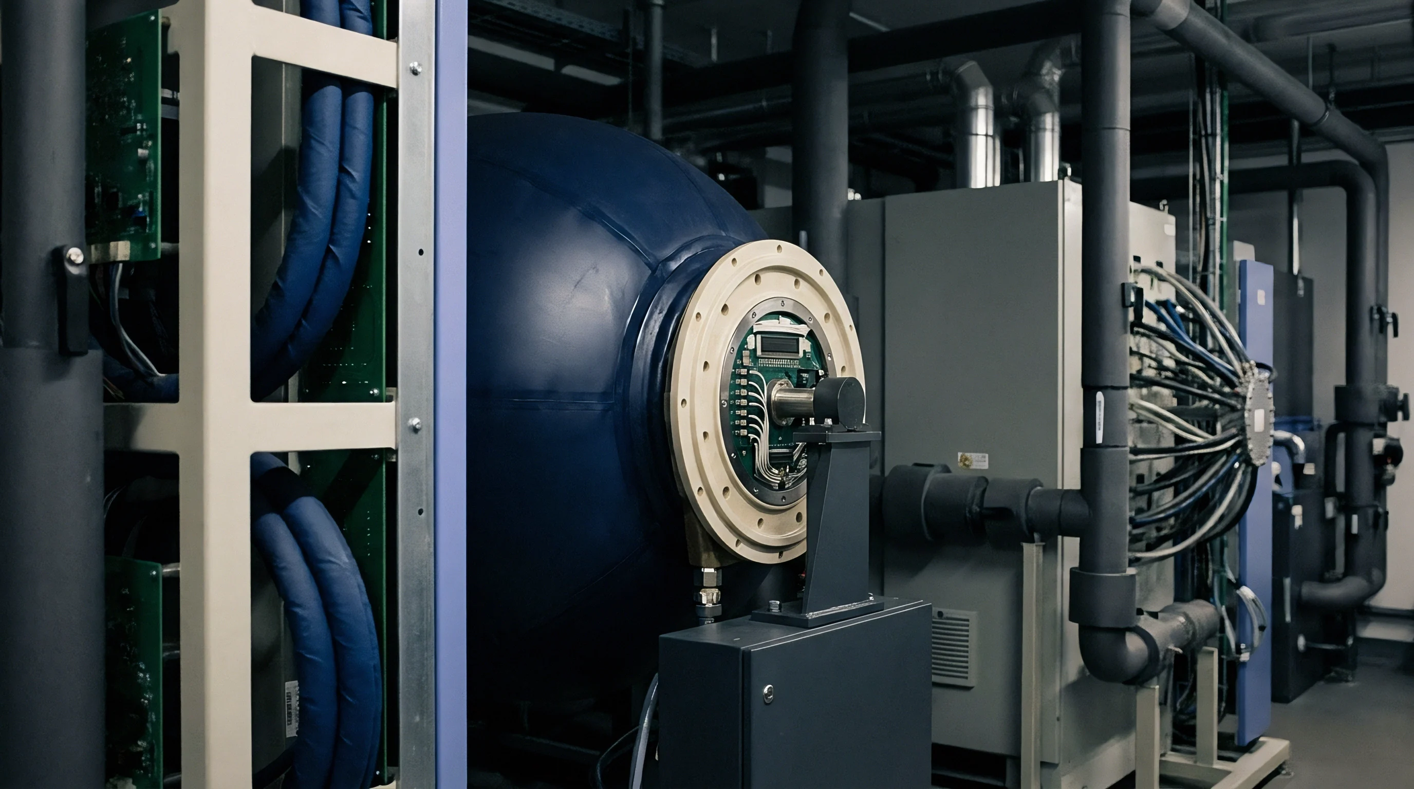
Thermal environmental chambers used in sensor characterization rely on forced air circulation to maintain internal thermal equilibrium. Air movement across sealed test enclosures forms boundary layers over circuit boards that alter local heat dissipation rates. While standard test specifications call for temperature uniformity within tight boundaries, local velocity variations create microclimates around individual packages.
A sensor mounted near the intake duct experiences convection rates distinct from a part near the exhaust recirculation path. These convective differences pull internal micro-electromechanical systems (MEMS) silicon die temperatures away from the control thermocouple reading, corrupting baseline thermal coefficients.
Convective heat transfer inside test volumes operates under mixed flow regimes where local air speed directly drives heat transfer rates. Increasing fan speed to minimize gross spatial gradients can backfire: high-velocity air streams create turbulent eddies around test cards, driving transient temperature fluctuations across packaged accelerometers. Silicon proof-mass structures respond to these thermal fluctuations through mechanical deformation and internal stress redistributions.
High air velocity accelerates surface heat transfer, whereas stagnant air pockets delay the time required for a device die to reach thermal equilibrium with the chamber setting.
Air velocity exceeding two meters per second inside a soak chamber introduces localized micro-convective cooling that shifts MEMS silicon die temperatures up to zero point four degrees Celsius away from the reference sensor reading.
Spatial temperature distribution in an empty chamber differs significantly from the profile observed in a fully loaded enclosure. Aluminum fixtures, card cages, and cabling bundles alter internal duct geometry, shifting uniform laminar streams into complex flow paths around physical obstructions. Thermal gradient mapping with multi-point resistance temperature detector arrays reveals spatial offsets between individual test sockets even under steady-state conditions.

Airflow Dynamics and Thermal Boundary Layers
Chamber duct configurations govern the boundary layer thickness formed over mounted printed circuit boards. Thin boundary layers from turbulent flow increase convective coupling between circulating air and integrated circuit packages, while thicker boundary layers under laminar flow reduce thermal coupling speed, extending the time required to settle at target temperatures. The resulting mechanical stress fields modify the piezoresistive or capacitive transduction mechanics governing proof-mass position sensing.
Standard calibration procedures require mapping internal velocity profiles across every test shelf before collecting characterization data.
Radiative heat transfer between interior chamber walls and test fixtures introduces additional thermal offsets. Interior chamber surfaces often exhibit emissivities distinct from aluminum fixture plates or FR4 circuit boards. During temperature transitions, chamber walls heat or cool faster than the circulating air volume.
Test devices positioned near interior walls absorb or radiate thermal energy directly to wall surfaces, bypassing convective air equilibrium. Reflective thermal shielding placed around the perimeter of the primary fixture array attenuates wall-to-device radiative coupling, isolating test devices within a uniform convective zone.
Reported temperature variations are often attributed to customer wiring fixtures rather than internal ducting turbulence.

Fixture
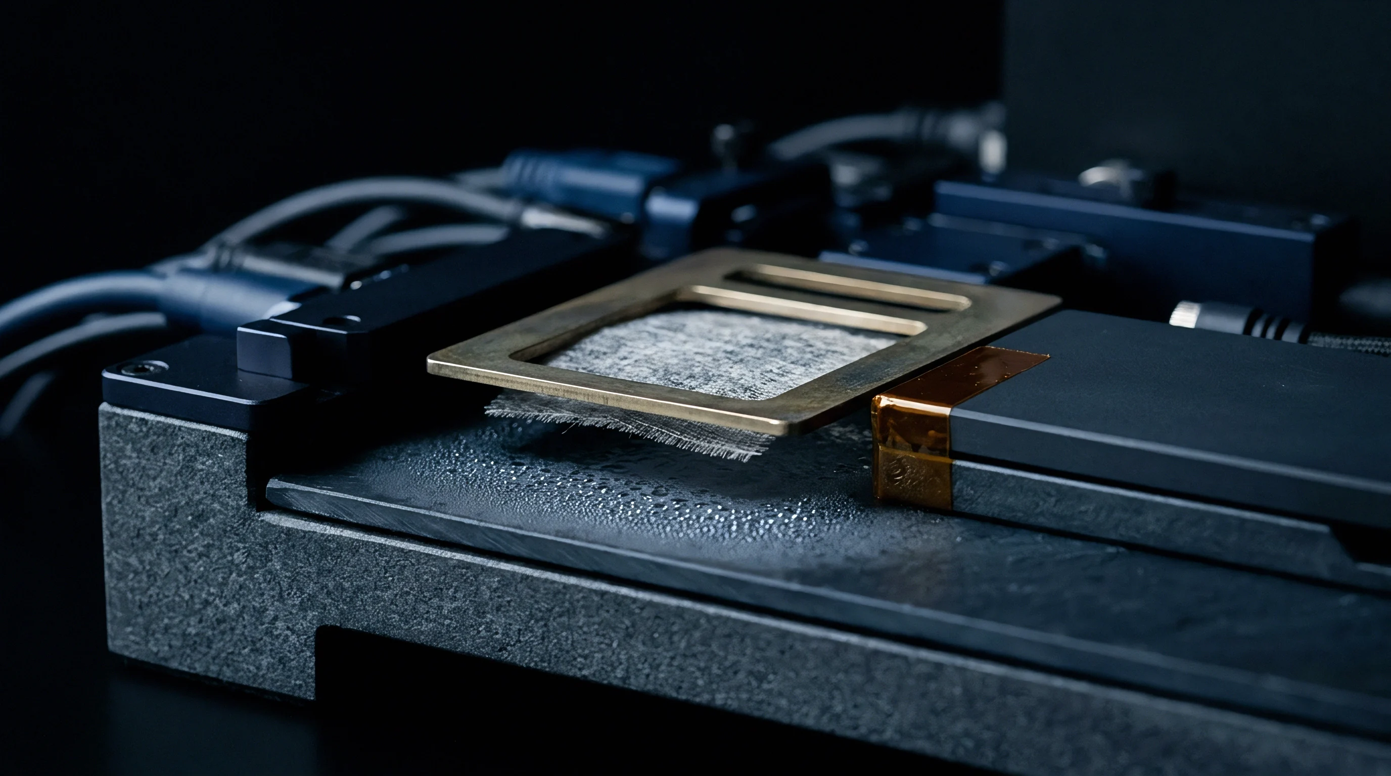
Structural mounting elements bridge the mechanical interface between the chamber test plate and the microelectromechanical die package. When a carrier board expands or contracts at a rate different from the silicon substrate or package ceramic, mechanical shear stress transfers directly into the MEMS sensor frame. Piezoresistive sensing elements convert this mechanical strain into false acceleration signals, generating an offset shift identical to physical motion.
Capacitive sensing elements experience changes in comb-finger spacing caused by frame distortion, altering both zero-g bias and scale factor calibration metrics.
Substrate material selection sets the baseline strain transfer behavior during thermal soak cycles. Standard FR4 glass-epoxy laminate exhibits a coefficient of thermal expansion ranging from fourteen to seventeen parts per million per degree Celsius, while monolithic silicon exhibits an expansion coefficient near two point six parts per million per degree Celsius. Mounting a silicon MEMS package directly to standard FR4 results in substantial thermo-mechanical stress across a wide operating temperature window.
High-reliability testing demands carrier substrates with expansion characteristics closely matched to the sensor package material.
| Substrate Material | Coefficient of Thermal Expansion (ppm/°C) | Thermal Conductivity (W/m·K) | Elastic Modulus (GPa) | Strain Transfer Propensity |
|---|---|---|---|---|
| Standard FR4 Epoxy | 14.0 to 17.0 | 0.3 to 0.5 | 22 | High |
| Polyimide High-Temp PCB | 12.0 to 15.0 | 0.4 to 0.5 | 25 | Moderate to High |
| Alumina Ceramic (Al2O3) | 6.5 to 7.2 | 24.0 to 30.0 | 330 | Low |
| Invar 36 Alloy | 1.2 to 1.5 | 10.5 to 13.0 | 140 | Very Low |
| Aluminum 6061-T6 | 23.0 to 24.0 | 167.0 | 69 | Severe |
Kinematic mounting designs isolate the sensor carrier board from structural deformation occurring in the primary chamber fixture plate. Machined aluminum fixture plates expand significantly over wide thermal sweeps; rigidly screwing a carrier circuit board across multiple attachment points transfers that thermal expansion into the board, warping the test substrate. Kinematic mounts using hardened steel pins resting in precision slots allow unconstrained thermal expansion of the carrier board while maintaining precise geometric orientation relative to the primary measurement axes.

Mechanical Strain Coupling in Package Substrates
Printed circuit board materials expand and contract in response to ambient environmental shifts, shifting the sensor zero offset. Designing carrier boards with localized strain-relief slots cutout around accelerometer package footprints mechanically decouples sensor leads from surrounding substrate flexure. Solder joint geometry plays an equally critical role in strain transmission: lead-free solder alloys exhibit high elastic moduli and susceptibility to thermal fatigue, transferring board-level stresses into package leads.
High-lead solders or conductive epoxy adhesives provide compliant interfaces that absorb differential thermal expansion without transmitting severe forces into the sensor enclosure.
- Die-attach strain coupling occurs when thermal expansion differences between the silicon die and package substrate transfer mechanical shear forces through the die-adhesive layer into the capacitive sensing element.
- Substrate flexure hysteresis develops when circuit board laminates undergo irreversible dimensional creep after repeating thermal cycling sweeps across maximum operating boundaries.
- Solder pad shear fatigue creates localized contact resistance changes and mechanical micro-shifts that manifest as sudden baseline offset jumps during dynamic thermal transitions.
- Kinematic pin binding arises when differential thermal expansion between steel guide pins and aluminum mounting plates creates mechanical friction, locking the test frame in a strained state.
Ignoring substrate expansion compatibility leads directly to corrupted thermal zero-g offset data, generating compensation coefficients that degrade measurement accuracy during final system operation.
Harness
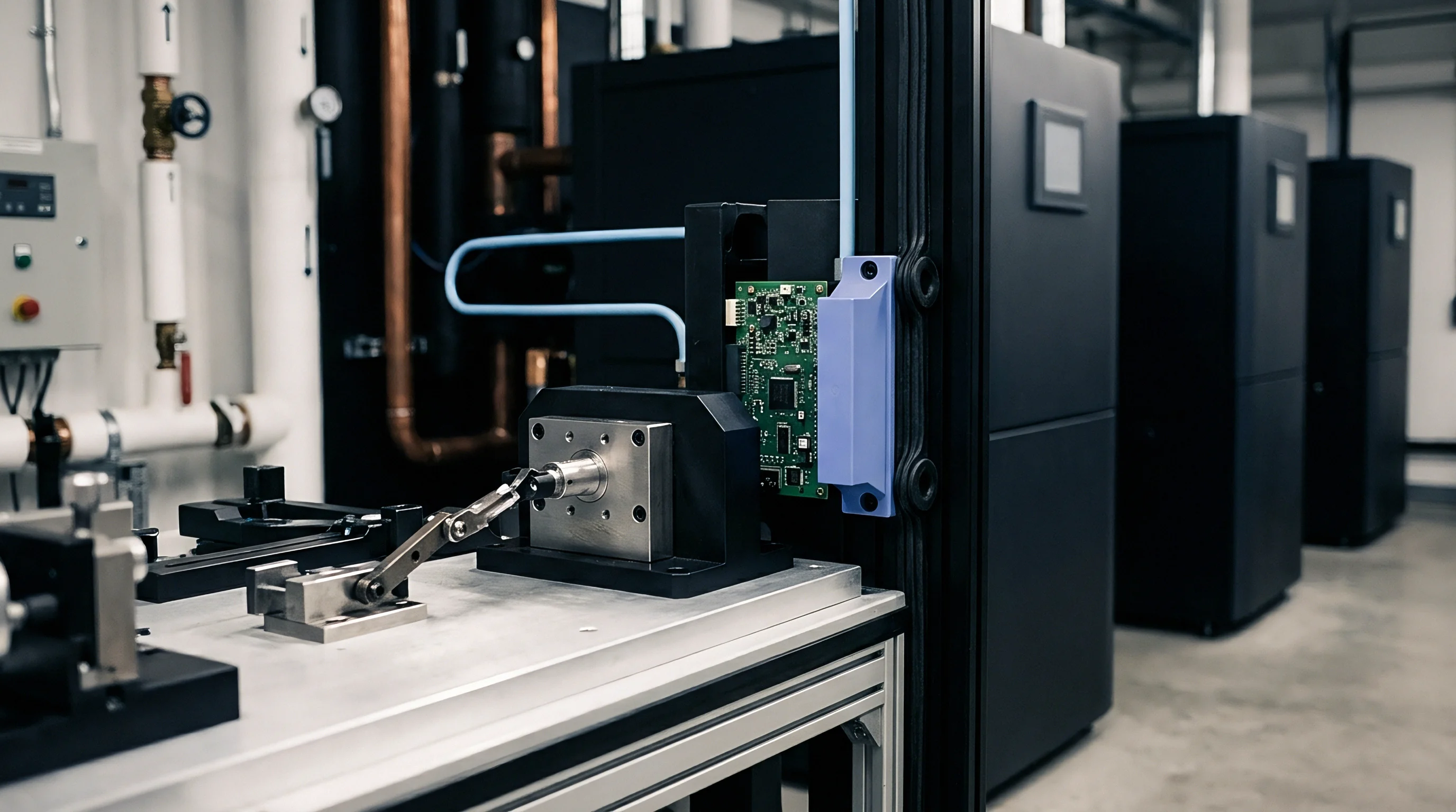
Electrical interconnections spanning the boundary between the internal test space and external instrumentation introduce unintended measurement corruption. Signal wires passing through chamber wall bulkheads form conductive thermal paths that carry ambient heat into test sockets, creating localized temperature gradients across device leads. Unshielded wiring bundles routed across forced-air fan assemblies pick up electromagnetic fields, corrupting low-amplitude analog sensor outputs before conversion.
Thermoelectric voltage generation presents a persistent measurement error inside thermal test chambers. Joining two dissimilar metals within a signal circuit creates a thermocouple junction that generates a temperature-dependent microvolt-level potential. Copper test leads soldered to Kovar or brass package leads form opposing thermal junctions.
Temperature gradients across the circuit board create unequal heating at these junctions, producing net DC offsets that shift as chamber temperature changes. Signal-chain designs call for symmetrical layout geometries to keep opposing thermal junctions at identical temperatures, canceling thermoelectric offset errors.
MIL-STD-883 Method 1010 dictates continuous parameter monitoring during thermal stabilization to prevent unrecorded signal transients from passing lot acceptance.
Cable insulation materials exhibit temperature-dependent dielectric properties that shift line capacitance during soak cycles. Fluorinated ethylene propylene and polytetrafluoroethylene retain stable dielectric constants across broad temperature sweeps. Standard polyvinyl chloride insulation demonstrates significant dielectric loss and capacitance shifts when heated, altering signal-chain filter characteristics.
Triboelectric noise generated by mechanical vibration of test cables against chamber walls introduces spurious AC signals into sensitive high-impedance nodes.

Parasitic Impedance and Thermoelectric Effects
Temperature variations along conductor pathways generate microscopic voltage differentials across dissimilar metal interfaces, while cable capacitance shifts with insulation temperature. Differential analog signals routed through low-noise shielded twisted pairs minimize external magnetic coupling while providing rejection of common-mode environmental noise. Shield grounds tied exclusively to a single reference point at the external data acquisition interface prevent ground loop currents across thermal boundaries.
| Cable Insulation Type | Dielectric Constant Shift (-40°C to +125°C) | Insulation Resistance at 125°C (MΩ/m) | Triboelectric Noise Susceptibility | Recommended Application |
|---|---|---|---|---|
| Standard PVC | 15.0% | High | External Non-Thermal Routes | |
| PTFE (Teflon) | 10,000 | Very Low | In-Chamber Signal Lines | |
| FEP Fluoropolymer | 8,000 | Low | In-Chamber Power and Ground | |
| Silicone Rubber | ~ 5.0% | ~ 500 | Moderate | Flexible Mechanical Interfaces |
Section four of the automotive sensor qualification specification voids all calibration data gathered over unshielded twisted pair lines exceeding thirty centimeters in length.
Hysteresis
Micro-electromechanical silicon sense elements retain physical memory of prior temperature exposures, causing thermal hysteresis that distorts accelerometer bias outputs. When an accelerometer transitions from cold temperatures to elevated operational limits and returns to ambient, zero-g bias readings rarely return to their exact initial state. Internal packaging materials, including epoxy die-attach adhesives and plastic molding compounds, experience visco-elastic stress relaxation during temperature transitions.
This relaxation alters residual mechanical stress imposed on the silicon die, shifting baseline output curves between rising and falling temperature sweeps.
Soak duration governs the thoroughness of mechanical equilibrium inside test packages, as necessary dwell times prevent uncompensated sensor lag. Fast ramp rates create substantial internal temperature gradients between the external package frame and the interior silicon structure. Silicon dies reach thermal equilibrium fast, but surrounding packaging materials require extended soak durations to relax mechanical strain completely.
Characterizing a sensor during rapid temperature ramping captures transient dynamic lag alongside static thermal drift, corrupting the static compensation matrix.
Calculating the true thermal time constant of a mounted sensor assembly requires evaluating both thermal resistance and thermal mass parameters. The equation defining thermal settling time takes the form:
τth = Rth · Cth
Here, Rth represents conductive and convective thermal resistance between the chamber air stream and the silicon die, while Cth represents the total heat capacity of the sensor package and local carrier board. Achieving zero point zero one percent thermal stabilization demands a soak duration of at least seven times the system thermal time constant (τth). Shortening soak times below this physical threshold leaves unrelaxed stress in polymer die-attach layers, manifesting as non-repeatable sensor bias drift during subsequent operational cycles.

Where Does Thermal Lag Corrupt Calibration Matrices?
Internal component packages stabilize at rates governed by substrate mass and thermal resistance. Rapid temperature transitions induce non-uniform thermal expansion across package layers. The resulting internal shear forces warp the MEMS proof-mass cavity, displacing stationary sense electrodes relative to movable springs.
When calibration software samples sensor outputs before structural relaxation completes, the recorded data reflects transient mechanical deformation rather than pure temperature-dependent drift. Compensation polynomials derived from incomplete soak cycles introduce systematic zero-g offset errors into final system navigation algorithms.
- Mount reference thermal sensors directly to carrier test substrates adjacent to accelerometer packages.
- Command chamber temperature transition from ambient to maximum operating temperature at controlled rate.
- Monitor die temperature output until drift drops below zero point zero five degrees Celsius per minute.
- Maintain thermal dwell for a minimum duration equal to five times the thermal time constant.
- Record baseline accelerometer bias output across ten consecutive measurement samples.
- Command chamber temperature transition down to minimum operating boundary at identical ramp rate.
- Execute matching thermal dwell time at lower temperature limit before taking cold baseline samples.
Whether internal die-attach polymers ever achieve complete mechanical stress equilibrium during continuous operational cycling remains unresolved across packaging research.

Residual
Mathematical modeling extracts systematic sensor drift patterns to establish baseline correction parameters. Accelerometer zero-g offset drift (Z0) and scale factor drift (S0) change continuously across temperature ranges. Signal conditioning circuits digitize raw sensor outputs, allowing onboard microcontrollers to apply polynomial compensation equations.
Residual calibration errors represent the difference between compensated sensor readings and true physical input accelerations across tested temperature limits.
Selecting polynomial order requires balancing curve-fitting accuracy against computational overhead. A first-order linear fit cancels primary temperature coefficients, but fails to compensate for non-linear silicon stiffness shifts and packaging stress curvature. Second-order quadratic models compensate for smooth non-linearities, significantly lowering residual bias errors across industrial temperature ranges (-40°C to +85°C).
Third-order polynomials reduce error further across wider automotive and aerospace envelopes (-40°C to +125°C). Higher polynomial orders risk overfitting measurement noise present in chamber baseline data, deteriorating performance between discrete calibration calibration points.
Third order polynomial compensation reduces thermal bias residuals by an order of magnitude compared to linear fit models.
Uncompensated thermal residuals degrade navigational accuracy, and these residual error limits determine overall sensor grade classification. High-performance MEMS accelerometers demand total uncompensated residual errors below five hundred micro-g RMS across the full operating range. Tactical-grade sensors demand residuals below fifty micro-g RMS.
Thermal soak test setups must maintain baseline measurement noise floors significantly lower than target residual error thresholds to avoid corrupting fitting parameters.
Polynomial Correction Models and Zero-G Offset
Second order algorithms cancel predictable sensor drift across operational temperature ranges, using offset calibration equations with discrete temperature terms to compute real-time bias corrections. The standard second-order compensation equation executes as follows:
acomp = fracaraw – (C0 + C1 · T + C2 · T2)S0 · (1 + S1 · T + S2 · T2)
Variable araw defines uncompensated acceleration, T indicates die temperature, C0 through C2 represent zero-g offset polynomial coefficients, and S0 through S2 define scale factor compensation terms. Coefficients derived from non-equilibrium soak test data yield imperfect matrices, amplifying uncompensated residual drift during real-world thermal transients.
| Transduction Principle | Raw Offset Drift (mg/°C) | Raw Scale Factor Tempco (ppm/°C) | Linear Fit Residual (mg RMS) | 2nd Order Residual (μg RMS) | 3rd Order Residual (μg RMS) |
|---|---|---|---|---|---|
| Capacitive Comb-Drive | 0.1 to 0.5 | 30 to 100 | 1.5 | 120 | 35 |
| Piezoresistive Beam | 0.5 to 2.0 | 150 to 500 | 4.2 | 450 | 110 |
| Resonant Silicon Beam | 0.01 to 0.05 | 5 to 20 | 0.3 | 15 | 4 |
| Thermal Convection MEMS | 0.2 to 0.8 | 100 to 300 | 2.8 | 280 | 85 |
Sensors calibrated using dynamic thermal ramps consistently display larger residual errors in application than those calibrated under true steady state soak conditions.
Outlay
Financial commitments required for sensor qualification testing depend directly on chamber stabilization speed and channel density. Thermal soak time sets throughput: extended thermal soak dwells guarantee accurate baseline coefficient generation, yet increase overall test duration per batch. Test facility operators balance qualification thoroughness against financial expenditure per production unit.
Capital investments for high-uniformity multi-zone thermal soak chambers run significantly higher than standard commercial environmental test chambers, driving operational cost overhead.
Longer thermal dwells reduce batch throughput. Testing hundreds of multi-axis MEMS sensors simultaneously requires dense fixture arrangements to maximize chamber efficiency. However, high-density arrays require expensive parallel data acquisition hardware, low-noise cabling, and automated switching matrices.
If channel density causes air stagnation within lower shelf volumes, yield drops due to uneven thermal settling across the batch. Scrapping or re-testing parts that fail residual error criteria due to fixture thermal gradients increases total landed component cost.

Capacity Sizing and Screening Economics
Production facility throughput drops sharply when thermal dwell times are extended to compensate for uneven chamber air distribution. Sourcing engineers evaluate chamber channel density against total cost per operational test hour. Investing in precision thermal fixtures with low heat capacity reduces thermal transition lag, shortening required soak times without compromising baseline data accuracy.
Automated temperature chamber integration allows continuous multi-point calibration execution, reducing labor expenses and maximizing equipment utilization across production cycles.
- Thermal recovery rate specification defines how fast a loaded test volume returns to setpoint stability after loading door cycles, directly impacting batch test run times.
- Channel density scaling balances total simultaneous sensor testing capabilities against high-speed data acquisition hardware costs and cabling layout complexity.
- Data acquisition synchronization ensures parallel sampling systems sample all active sensor channels simultaneously during defined thermal equilibrium windows.
- Chamber calibration maintenance establishes mandatory calibration schedules for internal temperature sensors, air velocity controllers, and fixture thermal monitors.
Allocating capital to custom carrier boards with matched thermal expansion properties reduces product scrap rates caused by artificial test strain. Optimizing thermal chamber airflow paths, fixture thermal mass, and low-noise interconnection harnesses establishes an effective baseline test environment. High-volume sensor qualification workflows depend on reliable thermal soak parameters to ensure delivered accelerometers meet datasheet bias and scale factor stability targets across full operational lifecycles.