Thermal Hysteresis Reduction in Silicon Capacitive Accelerometer Package Assembly
Compliant single-point die anchors and ceramic cavity packages eliminate thermal-mechanical strain hysteresis across automotive sensor operating temperatures.
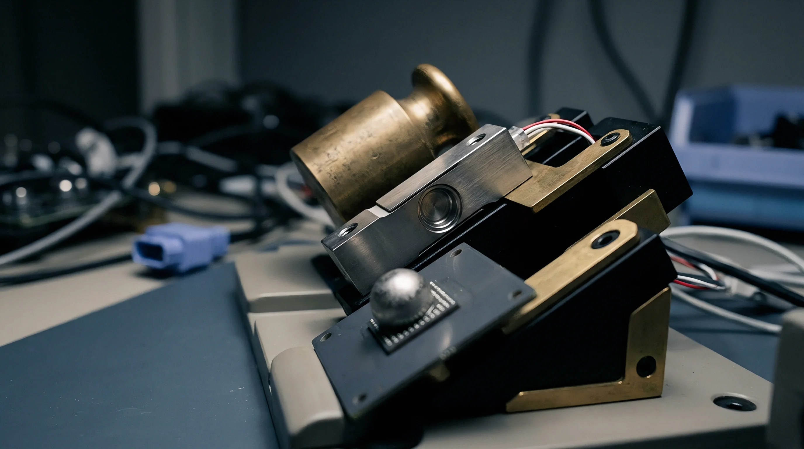

Strain
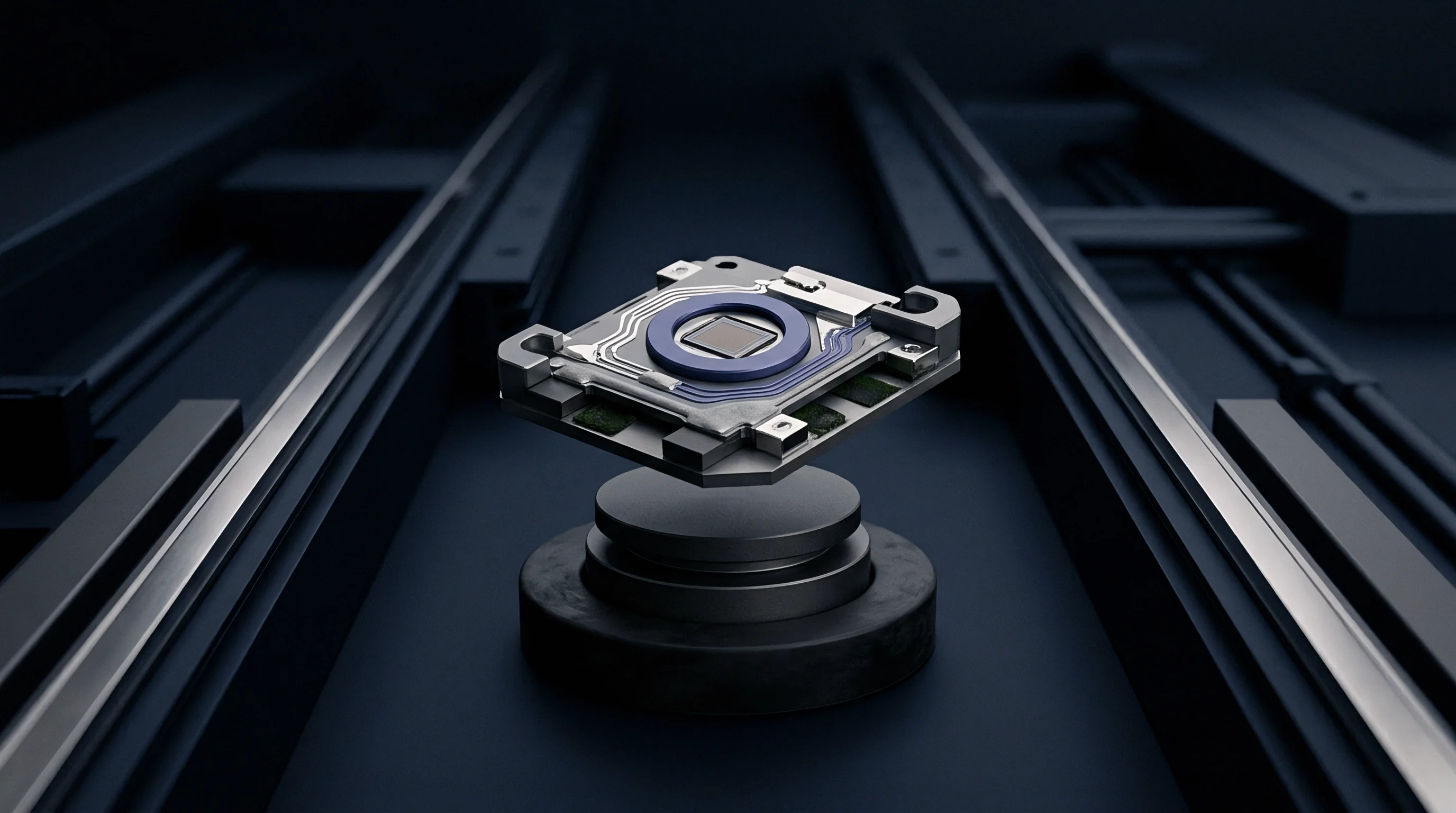
Transduction Dynamics under Thermal Expansion
In a silicon micro-electro-mechanical element, differential capacitance relies on micrometer-scale gaps between fixed and movable comb fingers. Moving the proof mass alters this baseline spacing, shifting the rest capacitance. However, thermal-mechanical stress from outside the micromachined structure can also deform the die surface, changing the distance between opposing finger arrays even without external acceleration.
Silicon itself expands linearly at roughly 2.6 parts per million per degree Celsius, but the structural materials attached to the die expand much faster, driving geometric distortion whenever temperature changes.
This expansion in silicon remains linear and predictable.
Across temperature cycles, zero-g offset drift follows two separate mechanical paths. Reversible elastic warping shifts capacitance symmetrically as temperatures rise and fall. Irreversible viscoelastic deformation, on the other hand, introduces path-dependent non-repeatability ~ the root of thermal hysteresis.
Polymer adhesives used in die mounting shift through distinct modulus regimes across their working temperature range. Below their glass transition temperature, high storage modulus transfers package flex directly into the sensor die. Above that threshold, structural relaxation lowers the storage modulus while raising the loss factor, tracing stress hysteresis loops during thermal sweeps.
A 100-micron silicone die-attach layer reduces stress transmission by 82 percent compared to rigid epoxy under a thermal ramp of 5 degrees Celsius per minute.
Where and how the die is anchored determines how internal stress spreads across the capacitive comb structure. Multiple attachment points along the die perimeter gather displacement vectors from the underlying substrate and transmit shear forces straight into the suspension springs. This mechanical input shifts the proof mass from its rest position relative to the frame, creating a differential gap shift that the analog front end reads as an acceleration signal.
Polyimide passivations and silicon oxide insulation layers add secondary stress through intrinsic film tension, compounding the package thermal mismatch.
The layout of these anchor points directly governs structural distortion.

Viscoelastic Mechanisms in Die Attach Interfaces
Under sustained load, polymer adhesives naturally creep.
Adhesive layers face continuous shear forces whenever temperatures cycle across assembly limits. Inside an organic polymer, stress relaxes at rates that depend on thermal ramp speed, dwell time at temperature extremes, and total moisture content. Heating the assembly quickly generates peak stress before the polymer structure can relax, whereas slower ramps allow energy to dissipate continuously.
Because this behavior depends on rate, simple temperature compensation routines fail, leaving uncorrected residual offset shifts at room temperature.
Unchecked thermal expansion degrades zero-bias stability.
Distortion in the internal sensing cavity creates cross-axis coupling alongside simple offset shifts. Uneven die warping tilts the proof mass away from its primary plane of motion, introducing out-of-plane capacitance changes into the main sensing channel. Evaluating package stress typically traces structural degradation to specific physical mechanisms:
- Glass Transition Shift alters storage modulus by two orders of magnitude, converting compliant support into rigid mechanical coupling during low-temperature exposure.
- Viscoelastic Shear Creep redistributes interfacial mounting stress unevenly during extended temperature dwell periods, preventing the die from returning to initial spatial coordinates.
- Anisotropic Substrate Flexure deforms the package base plane along unequal crystallographic axes, driving torsional twisting into single-ended suspension beams.
- Moisture Desorption Kinetics reduces polymer mass during high-temperature dwell, inducing volumetric contraction that shifts baseline zero-g output.
Ignoring viscoelastic strain transmission during package design leaves the assembly vulnerable to permanent zero-g offset shifts above 50 milli-g after environmental thermal cycling, invalidating factory calibration data.
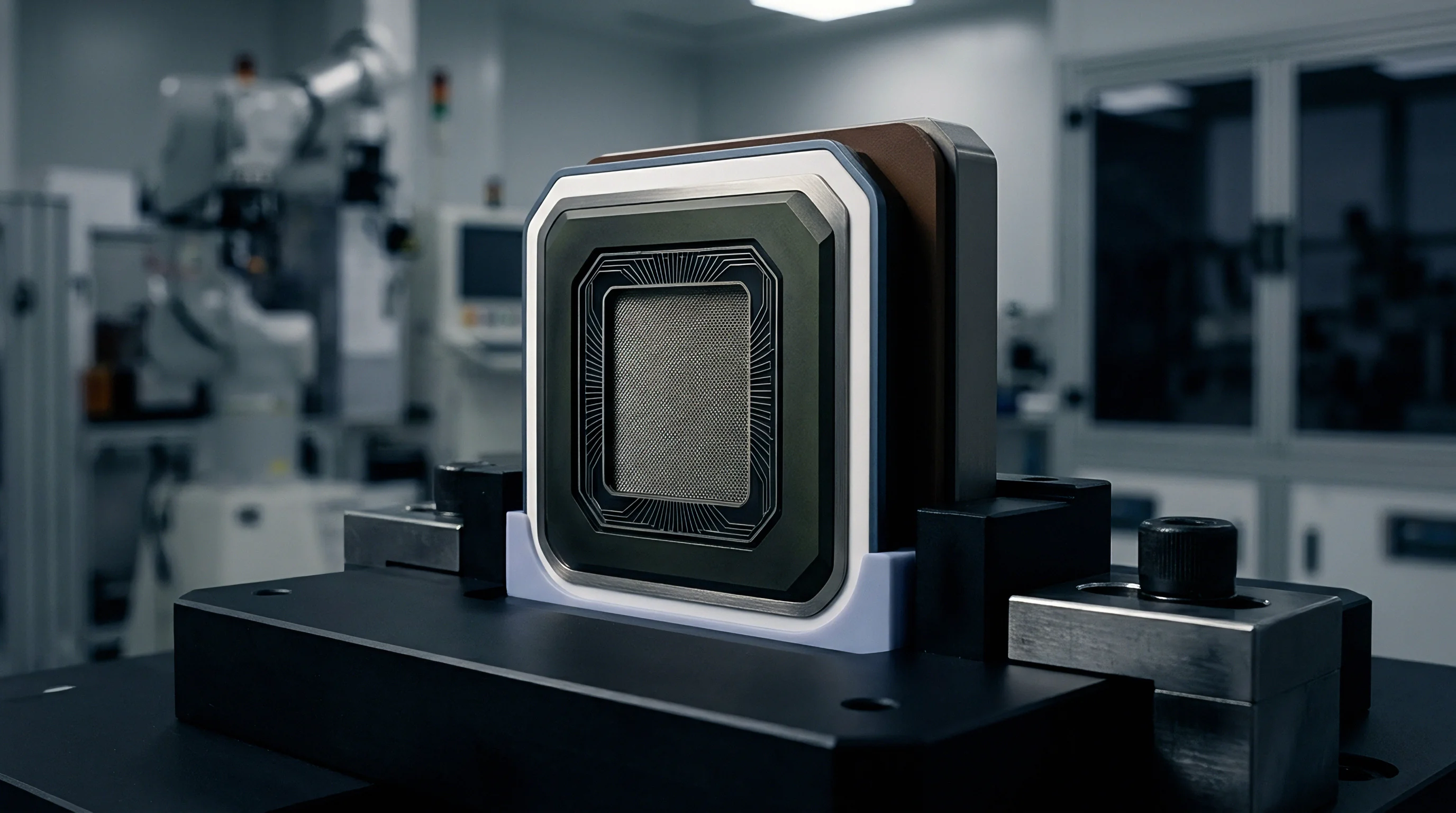
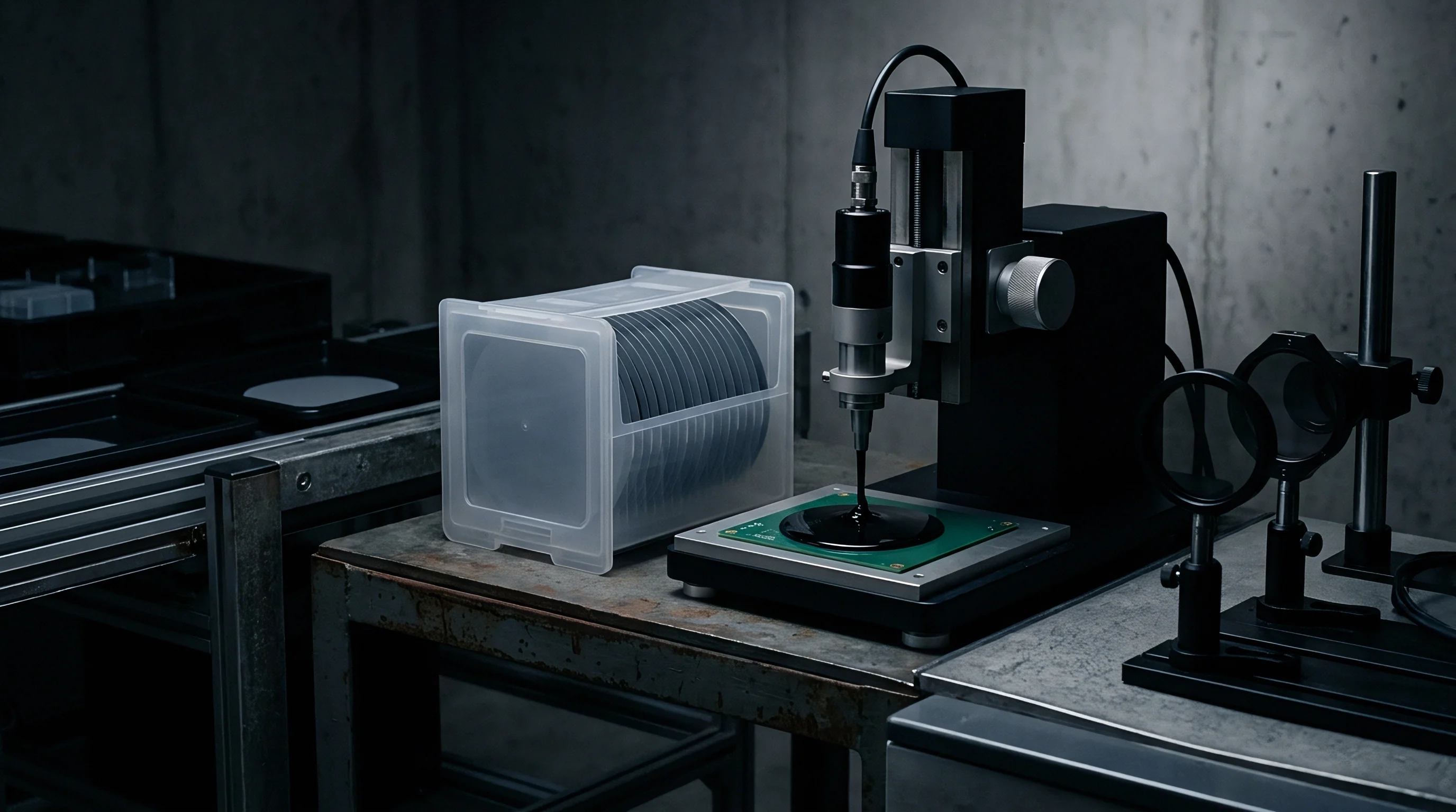
Substrate
Package Architecture and Mechanical Isolation
Package selection defines the mechanical environment around the micromachined element. Ceramic leadless chip carriers closely match silicon’s coefficient of thermal expansion at around 6.5 parts per million per degree Celsius, limiting dimensional divergence. Transfer-molded plastic quad flat no-lead packages expand faster ~ between 10 and 17 parts per million per degree Celsius ~ placing greater thermal strain on encapsulated components.
Plastic molding compounds touch the die surface directly unless a cavity layout isolates the internal microstructures.
Ceramic substrates come at a higher unit cost.
Cavity structures shield comb fingers from direct compressive molding stress. In an open-cavity ceramic format, ambient pressure remains constant while mounting forces transfer only through the die base interface. Transfer-molded plastic designs cover the silicon die in thermosetting epoxy resin.
As the compound cools after molding, thermal contraction exerts triaxial compression on the die edges, compressing the comb frame and biasing the suspension springs.
By preventing direct resin contact, cavity designs preserve comb gaps.
| Die-Attach Material | Substrate Format | Young Modulus (GPa) | Material CTE (ppm/°C) | Offset Hysteresis (-40 to 125°C) |
|---|---|---|---|---|
| Eutectic AuSn | Ceramic LCC Cavity | 68.0 | 16.0 | 12.5 mg |
| Silver-Filled Epoxy | Plastic QFN Molded | 8.5 | 35.0 | 45.0 mg |
| Flexible Silicone | Ceramic LCC Cavity | 0.005 | 300.0 | 1.8 mg |
| Patterned Polyimide | Organic Substrate Cavity | 3.2 | 40.0 | 18.2 mg |

Decoupling Structures and Mounting Topology
Compliant silicone relaxes thermal stress rapidly.
Single-point center anchoring isolates the active sensor layout from perimeter substrate expansion. Mounting the silicon die on a central pedestal restricts physical bond transfer to a tiny surface area directly below the proof mass center of symmetry. Thermal strain expands the surrounding substrate outward while the central pedestal holds the sensor frame neutral.
Four-corner adhesive bonding mounts the die across its full footprint, transmitting every vector of substrate flexure straight into the capacitive comb array.
By contrast, gold-tin solder yields high mechanical stiffness.
Placing silicon or glass interposers between the sensing element and package substrate creates an intermediate expansion gradient. A silicon interposer matches the MEMS element thermal expansion perfectly, absorbing shear stress across a sacrificial polymer bond layer below the interposer base. Structural decoupling performs best when assembly parameters reflect system-level operating conditions:
- Central Pedestal Mounting confines structural interface stress to the neutral axis of the sensor layout, attenuating edge-driven frame warping.
- Compliant Silicone Adhesives absorb mechanical substrate displacement through low-shear elastic strain, dampening thermal stress transmission.
- Patterned Adhesive Dispensing eliminates continuous bond lines, creating stress relief voids beneath non-critical die areas.
- Stress Isolation Grooves carved into the silicon substrate frame divert thermal wave propagation around suspension beam anchors.
Thick overmolding compounds are sometimes used to provide uniform hydrostatic pressure intended to stabilize internal comb structures across thermal cycles.

Process

Thermal Curing Profiles and Stress Relief Annealing
Thermal profiles during die bonding and molding establish the room-temperature stress state of the sensor assembly. Curing adhesives at high temperatures sets a zero-stress baseline at elevated thermal levels. As the completed assembly cools to ambient room temperature, differential contraction generates baseline strain.
Lowering cure temperatures reduces total thermal drop during cooling, decreasing residual assembly stress.
Unbalanced or asymmetric cure profiles warp die structures.
Absorbed moisture alters baseline polymer mass.
Controlled step curing lowers peak stress spikes inside organic polymers. A multi-stage thermal profile allows solvent evaporation at moderate temperatures prior to cross-linking at full polymerization levels. Fast single-stage curing traps volatile components within the adhesive matrix, forming micro-voids and non-uniform cross-link density.
These structural defects cause irregular stress distribution that degrades hysteresis stability during subsequent temperature cycling.
Adherence to IEC 60068-2-14 test condition Nb forces exposure to rapid temperature change without latent solder joint stress cracking.

Why Does Post-Mold Annealing Alter Long-Term Zero-G Stability?
Post-mold baking relaxes trapped mechanical strain inside thermosetting resins through molecular realignments. Transfer molding leaves non-uniform stress distributions across plastic QFN packages due to uneven cooling rates and flow geometries. Extended thermal annealing near the resin glass transition temperature accelerates structural stress relaxation, preventing unpredictable dimensional shifts during normal operational cycles.
Skipping post-mold bake steps exposes sensor assemblies to gradual zero-g baseline drift over months of operation.
- Pre-bake package substrates at 125 degrees Celsius for 4 hours to eliminate absorbed environmental moisture prior to die attachment.
- Dispense compliant silicone adhesive using dot matrix geometry to guarantee uniform thickness without air entrapment.
- Execute ramped adhesive curing starting at 80 degrees Celsius and elevating to 150 degrees Celsius over a 120-minute window.
- Perform high-temperature storage annealing at 150 degrees Celsius for 24 hours to stabilize polymer stress relaxation before electrical calibration.
Standard quality documentation specifies that any deviation from the thermal ramp rate limits detailed in IEC 60068-2-14 test condition Nb renders factory thermal hysteresis calibration void.

Yield
Calibration Boundaries and Compensation Limitations
Temperature compensation networks inside integrated signal conditioning ASICs utilize polynomial equations to correct zero-g bias shift. Third-order and fourth-order polynomial math matches smooth offset curves across broad temperature ranges. Polynomial compensation fails to correct thermal hysteresis due to the path-dependent nature of viscoelastic relaxation.
Heating the sensor along a specific thermal path yields different capacitance values than cooling along the identical temperature curve.
Firmware compensation alone misses rate-dependent effects.
Internal temperature gradients distort transient readings.
Thermal lag between the internal sensing element and external compensation thermistors introduces transient measurement errors. Rapid ambient temperature swings heat the package exterior while the internal silicon proof mass lags behind. Internal signal conditioning circuits applying thermistor-based mathematical corrections read incorrect die temperature data during fast thermal transients, introducing temporary output spikes.
Anchoring a silicon MEMS element at its geometric center isolates the comb fingers from perimeter die expansion.
| Package Construction | Thermal Hysteresis Loop Width (-40 to 125°C) | Transient Thermal Gradient Error | Post-Calibration Residual Bias Drift |
|---|---|---|---|
| Plastic Overmolded QFN | 38.2 mg | 14.5 mg/(°C/min) | 8.2 mg |
| Plastic Cavity QFN | 12.4 mg | 5.1 mg/(°C/min) | 2.8 mg |
| Ceramic LCC Perimeter Bond | 9.8 mg | 4.2 mg/(°C/min) | 2.1 mg |
| Ceramic LCC Center Pedestal | 1.2 mg | 0.8 mg/(°C/min) | 0.4 mg |

Verification Testing and Qualification Protocols
Production screening for thermal hysteresis requires complete thermal cycling sweeps inside environmental test chambers. Test setups evaluate sensor outputs across multiple temperature steps, measuring difference values between ascending and descending thermal paths at identical stabilization points. Dwell times at test temperatures must allow complete thermal equalization through the package core.
Verification documentation requires specific parameters to validate thermal stability performance:
- Thermal Sweep Hysteresis Curves plotting zero-g output drift across minimum three consecutive full-range heating and cooling loops.
- Rate-Dependent Transient Profiles recording output variance under thermal ramp speeds ranging from 1 to 10 degrees Celsius per minute.
- Long-Term Bake Stability Records proving zero-g bias shift remains within specified boundaries following 1000 hours at maximum operating temperature.
- Moisture Sensitivity Qualification Reports measuring offset stability shifts before and after soak testing under JEDEC J-STD-020 standards.
How much thermal hysteresis can be economically removed via multi-point temperature calibration before additional assembly hardware costs outweigh testing time investments?
Supply

Supplier Pool Structure and Manufacturing Logistics
Sourcing low-hysteresis capacitive MEMS accelerometers requires evaluating both wafer foundry capabilities and packaging assembly expertise. Standard OSAT providers often utilize high-volume transfer molding lines optimized for logic microcontrollers, applying aggressive mold compound formulations that generate heavy thermal-mechanical stress. Specialized sensor assembly houses maintain dedicated cavity-packaging lines, compliant silicone dispense systems, and long-duration thermal annealing ovens designed specifically for MEMS stress isolation.
While plastic overmolding lowers assembly costs, it raises stress.
Effective dual sourcing requires matching the package thermal footprint.
Automotive applications compliant with AEC-Q100 Grade 0 require rigorous environmental stress testing across -40 to 150 degrees Celsius. Meeting these standards limits the available packaging options to hermetic ceramic cavity structures or specialized stress-decoupled cavity QFN packages. High-grade industrial instrumentation favors ceramic LCC formats despite higher unit production costs, avoiding long-term warranty expenses driven by zero-bias drift.
Hermetic ceramic packages eliminate moisture desorption cycles that skew capacitive readings across thermal ramps.
Selecting compliant silicone die-attach materials over conventional silver-filled epoxy increases package thermal isolation while extending production cycle times due to lower temperature curing schedules.