MEMS Capacitive Accelerometer Zero Offset Drift Calibration Fundamentals
MEMS capacitive accelerometer zero offset drift stems from package strain hysteresis, charge trapping, and thermal creep, requiring multi-axis tumble calibration and polynomial compensation.


Die
Differential capacitance variations down to single-attofarad levels govern the acceleration response in surface-micromachined silicon elements, where mechanical symmetry dictates output stability. At zero acceleration on a level bench, suspension springs are designed to hold identical air gaps between the movable proof mass fingers and the fixed sensing electrodes. In practice, residual stress gradients through the polysilicon structural layers produce out-of-plane beam warpage, pulling the structure away from its geometric center.
Uncalibrated test benches routinely show a baseline offset between 20 mg and 100 mg at 25°C, which drifts further whenever the thermal load changes.
Micromechanical Sources of Bias Unbalance
Inside the MEMS cavity, structural imbalance shows up as uneven finger gaps, etched sidewall taper variations, and differential anchor stiffening. Comb-drive capacitance follows a parallel-plate model where capacitance is inversely proportional to gap width. Consequently, a sub-nanometer error along the primary 1.5-micrometer sensing gap unbalances the differential bridge and creates a raw zero-g bias.
Polysilicon grain boundaries also pin residual stress during high-temperature chemical vapor deposition and chemical-mechanical planarization. As these internal strains relax over time, the suspension beams’ mechanical neutral axis shifts, driving permanent baseline drift without any applied force.
Uncompensated zero-g offset voltage in differential capacitive sensing elements scales in direct proportion to structural beam thickness variations across the wafer die.
Electrostatic Parasitics and Anchor Stress
Electrical bias paths introduce parasitic forces directly onto suspended proof mass assemblies. Direct-current polarization voltages across differential sense capacitors generate continuous electrostatic attraction. Asymmetric trace routing creates subtle voltage imbalances between opposing comb arrays, exerting net static forces that displace the proof mass during zero acceleration conditions.
Silicon substrate anchors transmit package-level mechanical strain directly into suspension spring roots. Mounting strain distorts tether geometry, altering effective spring constants across orthogonal axes and moving the zero-g equilibrium position during board-level temperature excursions.
Uncompensated initial offset stems primarily from post-packaging stress relaxation, and board-level reflow profiles alter the mechanical boundary conditions enough to invalidate factory calibration trims.


Hysteresis
Thermal excursions expose micro-mechanical relaxation behaviors that shift baseline readings across repeated temperature cycles. When an assembly ramps from negative 40°C to positive 125°C and returns to room temperature, the zero-g output voltage rarely retraces its original path. Plastic mold compounds expand and contract at rates markedly different from monocrystalline silicon structures, with thermal expansion coefficients spanning 2.5 parts per million per degree Celsius for silicon up to 15 parts per million per degree Celsius for epoxy resins.
Solder reflow aggravates this mismatch, driving strain into the substrate mounts that persists long after the device reaches thermal equilibrium.

Thermal Cycle Memory in Molded Packages
Polymer matrix relaxation drives time-dependent baseline creep inside plastic-encapsulated surface-mount sensors. Epoxy mold compounds absorb ambient atmospheric moisture, altering structural elasticity and increasing total mass. Hydration expands the plastic frame, applying compressive forces to die perimeter bonds.
Drying cycles reverse this expansion unevenly, leaving structural stress fields altered. Ceramic leadless chip carriers mitigate polymer moisture absorption, maintaining tighter stress boundary conditions across wide operational temperature ranges.
Package stresses couple directly into the die through its anchor points, where silicon creep degrades offset stability over time. The structural interface between the die attach adhesive and the ceramic substrate absorbs shear strain, shielding central suspension tethers from localized housing compression. Specifying a low-stress silicone die attach instead of a rigid epoxy formulation substantially curtails this transmitted mounting strain.
| Package Type | Substrate Material | CTE Mismatch (ppm/°C) | Initial Zero Offset (mg) | Thermal Hysteresis Offset (mg) | 10-Year Long-Term Drift (mg) |
|---|---|---|---|---|---|
| Plastic LGA (3×5 mm) | FR-4 / Epoxy Compound | 12.5 | ±50 to ±100 | ±15.0 | ±35.0 |
| Plastic QFN (4×4 mm) | Copper Leadframe / Epoxy | 14.0 | ±40 to ±80 | ±12.0 | ±28.0 |
| Ceramic LCC (14-pin) | Alumina (Al2O3) | 4.2 | ±15 to ±30 | ±2.5 | ±6.0 |
| Hermetic TO-8 Metal | Kovar / Glass Seal | 3.0 | ±5 to ±15 | ±0.8 | ±1.5 |

Dielectric Charge Trapping Dynamics
Insulating layers in MEMS devices collect stray charge during extended operation. Silicon dioxide isolation pads situated beneath high-voltage actuation or sense lines trap migrating free electrons at dielectric interfaces, skewing the zero-g output. This trapped charge builds up parasitic electrostatic fields that pull the comb fingers toward substrate contacts, introducing fixed offsets that vary with operating voltage and ambient humidity.
Thermal hysteresis loops in plastic-packaged accelerometers stem from viscoelastic creep in die attach adhesives rather than monocrystalline silicon spring deformation.
Failing to isolate package-induced thermal hysteresis from sensor die drift results in over-compensating steady-state thermal coefficients, causing field failures where zero-g offset errors trigger false tilt detection during ambient temperature transitions.


Chamber
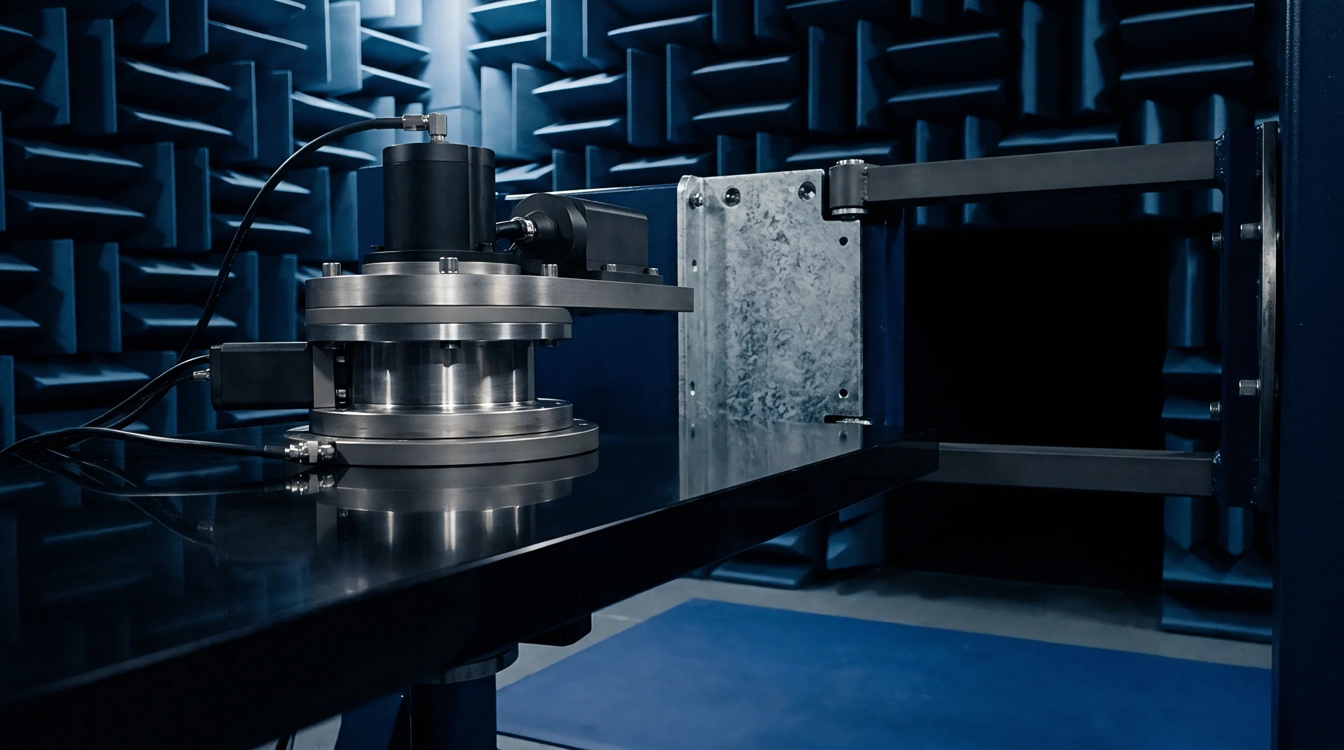
Environmental chambers supply the controlled conditions required to separate gravitational vectors from internal sensor bias. Mounting a triaxial module onto a precision motorized two-axis tilt table inside the chamber allows systematic mapping of zero-g offsets across all three orthogonal axes against local Earth gravity. Because internal thermal gradients immediately corrupt these static offset measurements, the chamber must hold temperature steady throughout each measurement dwell.

Six Position Orientation Calibration Procedure
Execution of a full tumble calibration requires controlled static holding periods at specific angular orientations. The sequence isolates individual axis bias from sensitivity scale factors by solving system linear equations.
- Mount the unit under test onto a precision aluminum fixture inside the thermal test enclosure, ensuring mechanical coplanar contact surfaces.
- Stabilize the enclosure internal temperature at the initial thermal test point for 45 minutes to eliminate thermal gradients across the sensor package.
- Rotate the test fixture to position the Z-axis pointing vertically upward, recording static output voltage over a 60-second window.
- Invert the fixture 180 degrees to align the Z-axis vertically downward, recording the inverted static voltage baseline.
- Index the fixture through X-axis positive, X-axis negative, Y-axis positive, and Y-axis negative orientations, capturing output streams at each hold point.
- Process static voltage arrays through a least-squares fit algorithm to calculate individual axis zero-g offsets and linear scale factors.
- Ramp the enclosure temperature to the next set point at 2°C per minute, repeating the orientation measurement matrix upon thermal stabilization.

How Does Gravitational Vector Realignment Isolate Cross-Axis Offset Errors?
Summing antiparallel gravity measurements cancels the true acceleration component, leaving the sensor’s raw internal bias. Running this routine across multiple temperature setpoints captures the bias drift curves needed for firmware compensation tables, though thermal hysteresis will warp simple polynomial fits, and in-band noise density sets a hard limit on calibration resolution.
| Calibration Step | Physical Variable | Target Range | Primary Error Mechanism | Residual Uncertainty |
|---|---|---|---|---|
| Spatial Alignment | Fixture Orthogonality | ±0.005 degrees | Machining Tolerance / Wear | 0.08 mg |
| Thermal Stabilization | Soak Time | 30 to 60 min | Internal Temperature Gradients | 0.15 mg |
| Gravity Reference | Local Acceleration g | 9.80665 m/s² | Geodetic Latitude Variance | 0.02 mg |
| Data Acquisition | ADC Resolution | 24 bits | Quantization & In-band Noise | 0.05 mg |
ISO 16063-21 Clause 5.3 mandates that primary low-frequency acceleration sensitivity matrix estimation must maintain a mounting torque uncertainty under 0.05 Nm to prevent fixture bending from introducing parasitic 2 mg bias offsets into calibration registers.

Arithmetic
Firmware routines running on the microcontroller subtract thermal bias drift in real time before sending acceleration data to the application layer. Digital signal processors convert raw counts into engineering units via mathematical correction functions, reading on-die temperature sensors directly from the silicon substrate while balancing accuracy against the non-volatile memory required for large lookup tables.
Polynomial Drift Estimation Structures
Mathematical modeling of thermal drift relies on polynomial functions up to the third order. Standard zero offset compensation equations follow structured formulations:
A_corrected = (A_raw – Offset(T)) / Sensitivity(T)
Offset(T) = a_0 + a_1 (T – T_ref) + a_2 (T – T_ref)² + a_3 (T – T_ref)³
Parameters a_0 through a_3 represent calibration coefficients derived from bench tumble tests. Constant a_0 sets baseline zero-g offset at reference temperature T_ref. Linear term a_1 accounts for steady-state thermal coefficient drift.
High-order terms a_2 and a_3 model non-linear thermal expansion behaviors and packaging stress shifts occurring at temperature extremes.
Applying a third-order temperature polynomial reduces zero-g offset drift from ±50 mg down to ±2 mg across a -40°C to +105°C operating span.

Kalman Filter State Formulations for Online Bias Tracking
Dynamic estimation filters track low-frequency offset drift during long mission profiles where periodic physical re-calibration is impossible. In these implementations, discrete-time Kalman filters treat zero-g bias as a stochastic random-walk state alongside velocity and position, capturing baseline shifts from packaging stress relaxation and sudden offsets caused by mechanical shocks.
Evaluating fixed-point mathematical structures against floating-point engines involves clear trade-offs across micro-controller architectures:
- Polynomial Curve Fitting consumes minimal flash memory while providing deterministic execution times across static operating profiles.
- Lookup Table Interpolation avoids complex floating-point math units by storing pre-calculated correction values in non-volatile memory arrays.
- Extended Kalman Filtering tracks dynamic zero offset drift caused by component aging but demands continuous high-speed processing budgets.
- Piecewise Linear Mapping reduces computational overhead in basic microcontrollers by connecting discrete calibration points with linear segments.
Polynomial temperature compensation tables calibrated only during rising thermal ramps introduce offset errors when ambient operating temperatures decrease.
Verification
Evaluating long-term drift performance demands statistical time-series measurement methods capable of separating random white noise from systematic sensor bias instability. Standard bench testing involves acquiring continuous zero-g output data in a vibration-isolated, thermally stabilized chamber over 100 consecutive hours. Standard noise metrics fail to isolate low-frequency bias fluctuations, necessitating specialized time-domain signal processing routines.

Allan Variance Signal Diagnostics
Plotting Allan deviation against cluster integration time on logarithmic axes separates the sensor’s competing noise mechanisms. Below one second, thermomechanical Brownian noise dominates as a velocity random walk, establishing a negative one-half slope. Between 10 seconds and 100 seconds, the curve flattens into a local minimum that defines the bias instability floor.
| Noise Region | Log Slope | Physical Mechanism | Industrial Target | Tactical Grade Target |
|---|---|---|---|---|
| Velocity Random Walk (VRW) | -0.5 | Thermomicro-mechanical Brownian Noise | 100 µg/√Hz | 10 µg/√Hz |
| Bias Instability (BI) | 0.0 | Flicker Noise / Charge Trapping | 0.5 mg | 0.01 mg |
| Rate Random Walk (RRW) | +0.5 | Temperature Gradient Fluctuations | 0.05 mg/√hr | 0.002 mg/√hr |
| Ramp Drift | +1.0 | Long-Term Packaging Strain Creep | 0.2 mg/day | 0.005 mg/day |

Aging Models for Extended Operational Lifespans
Extrapolating multi-year zero offset stability involves applying logarithmic time aging models derived from accelerated thermal stress testing. Exposing sensor lots to 125°C for 1,000 hours simulates ten years of room-temperature operational storage. Stress relaxation inside silicon structures follows standard time-dependent models where drift magnitude scales proportionally with the natural logarithm of operating hours.
A continuous 100-hour Allan variance profile at constant 25°C identifies the fundamental bias instability floor where digital filtering can no longer improve sensor resolution.
System designers face recurring risk when selecting zero offset compensation strategies for harsh environmental applications:
- Uncompensated Solder Creep shifts board-level mechanical stress boundaries, invalidating factory zero-g calibration values within months of field assembly.
- Die Attach Degradation introduces non-linear thermal drift paths that exceed second-order polynomial correction limits over extended thermal cycling.
- High-G Shock Events cause minor structural mechanical deformation in micro-scale suspension beams, shifting baseline offsets permanently.
- Supply Voltage Variations introduce offset errors when low-dropout regulator output voltages drift across operational temperature ranges.
Whether atomic-level stress relaxation in silicon springs stabilizes after ten thousand thermal cycles or continues as a permanent logarithmic creep remains unresolved in high-reliability sensing practice.