Differential Capacitive Bias Stability under Non-Uniform Substrate Thermal Fields
Spatial thermal gradients disrupt differential capacitive balance, requiring symmetric substrate layout and strain isolation to preserve bias stability.

Asymmetry
Differential capacitive sensing relies on geometric and dielectric parity between two complementary transducer elements. When a localized thermal gradient crosses a silicon die or ceramic base, this structural parity collapses. Heat flowing laterally across a differential pair establishes a temperature variance between sensing gaps, altering the relative permittivity of encapsulated gas or solid dielectric layers while expanding one capacitive structure faster than its neighbor.
In high-precision MEMS accelerometers, capacitive pressure sensors, and electrostatic inclinometers, spatial thermal imbalances generate an offset voltage indistinguishable from an physical input signal.
Standard common-mode rejection mechanisms fail under spatial thermal fields because common-mode suppression assumes isothermal temperature shifts across the entire sensor core. When an external component such as a power transistor, processing unit, or solenoid draws current and emits heat, thermal conduction through substrate traces creates a stationary or transient temperature gradient across the sensing element. A temperature difference as small as 0.05 Kelvin across a 2-millimeter differential MEMS structure induces a bias shift that exceeds the noise floor of twenty-bit analog-to-digital converters, destabilizing long-term zero-point accuracy.

Thermal Coupling Mechanisms in Differential Microstructures
Heat transfer across a micro-electro-mechanical substrate occurs through three parallel pathways: solid conduction through the bulk material, gas conduction across micro-gaps, and thermal radiation between stationary combs and proof masses. Solid thermal conduction through silicon or glass substrates dominates heat flux in sealed packages. Silicon exhibits a thermal conductivity near 148 Watts per meter-Kelvin at room temperature, which allows heat to move quickly but creates localized thermal stress concentrations when bound to materials with differing thermal expansion coefficients.
Dielectric permittivity within the capacitive cavity changes dynamically with localized temperature fields. For dry air or nitrogen cavity fill, the temperature coefficient of dielectric constant remains low, but thermomechanical deformation of the inter-electrode gap produces dominant bias errors. Differential capacitive balance requires that the baseline capacitance values under zero excitation remain matched within strict absolute tolerances across the operational temperature range.

Non-Uniform Thermal Drift Pathways
The gap spacing between fixed and moving electrodes varies locally as a function of thermal expansion and substrate warping. When heat enters from the left edge of a differential capacitive die, the left capacitive gap compresses or expands based on local structural anchors, while the right capacitive gap remains at a lower temperature and baseline geometry. The differential output signal, which processes the normalized ratio of capacitive differences over capacitive sums, registers a non-zero net charge.
A lateral thermal gradient of 0.1 Kelvin per millimeter across a silicon capacitive element generates an uncompensated bias drift equivalent to 12 milligravities of false acceleration.
Thermally driven gas displacement within hermetically sealed cavities adds a secondary drift mechanism. Spatial temperature fields induce gas density gradients across tiny micro-gaps, altering local damping coefficients and permittivity distributions. Ignoring lateral heat paths during transducer packaging leads directly to sensor baseline instability that calibration algorithms cannot isolate without dense localized temperature sensor arrays.


Swell
Volumetric deformation and structural flexure beneath a transducer die introduce mechanical strain fields that mimic mechanical measurands. Substrate warping alters the spatial alignment between anchored capacitive plates and suspended proof masses. When packaging materials undergo non-uniform thermal expansion, the die-attach layer experiences differential shear stress, transferring localized mechanical bending moments directly into the active silicon structure.
Die-attach materials such as conductive epoxies, eutectic alloys, and sintered silver pads exhibit distinct thermal expansion behaviors. A local hot spot on a printed circuit board heats one corner of the sensor package, inducing localized swelling in the organic die-attach matrix. This asymmetric swelling forces the silicon substrate into a torsional bend, shifting fixed capacitive electrodes relative to the central suspended mass.

Thermomechanical Strain Coupling
The interaction between the thermal coefficient of expansion of the substrate, package base, and silicon die governs mechanical strain transmission. Silicon has a thermal expansion coefficient around 2.6 parts per million per Kelvin, whereas alumina ceramic sits at 6.5 parts per million per Kelvin, and FR-4 circuit boards range from 14 to 17 parts per million per Kelvin. Under a non-uniform thermal field, these mismatches create spatially variable bending radii across the die platform.
| Substrate Material | Thermal Conductivity (W/m·K) | Expansion Coefficient (ppm/K) | Youngs Modulus (GPa) | Gradient Strain Sensitivity (nm/K) |
|---|---|---|---|---|
| Single-Crystal Silicon | 148.0 | 2.6 | 130 | 0.12 |
| Fused Silica | 1.3 | 0.5 | 73 | 0.04 |
| Alumina Ceramic (96%) | 24.0 | 6.5 | 300 | 0.48 |
| Low-Temperature Co-Fired Ceramic | 3.0 | 5.8 | 120 | 0.62 |
| High-Tg FR-4 Epoxy Laminate | 0.3 | 14.0 | 22 | 2.10 |
High thermal conductivity in single-crystal silicon minimizes internal thermal gradients but elevates mechanical stress transfer from low-conductivity packaging substrates. Conversely, materials like fused silica feature low expansion coefficients, isolating the sensing microstructures from thermomechanical swell at the expense of higher local thermal gradients under asymmetric thermal loads.
Failure Modes under Spatial Thermal Fields
Non-uniform thermal exposure breaks the internal balance of differential sensing structures through distinct mechanical failure pathways:
- Anchor Point Displacement shifts the spatial baseline of fixed capacitive electrodes, introducing an uncalibrated electrostatic force offset.
- Die-Attach Delamination occurs along the high-temperature gradient edge, permanently altering the structural boundary conditions of the die mount.
- Comb Finger Tilting distorts out-of-plane capacitive symmetry, increasing cross-axis sensitivity and parasitic capacitance to ground.
- Stress-Induced Piezo-Capacitive Shift alters the effective dielectric boundary condition near anchor points due to local silicon strain fields.
Soft elastomeric die-attach adhesives absorb substrate strain but introduce viscoelastic creep over continuous thermal cycling.

Bridge
Front-end conditioning circuits convert sub-femtofarad capacitance shifts into quantifiable voltage variations using alternating-current excitation bridges and charge-sensitive amplifiers. In isothermal conditions, symmetrical bridge topologies switch charge across complementary sensing nodes, canceling carrier noise and environmental drift. Under localized thermal fields, phase delay shifts in front-end demultiplexing switches and temperature-dependent parasitic capacitances alter charge transfer balance, degrading common-mode rejection.
Charge amplifiers connected directly to differential sensing nodes feature input capacitance and leakage current behavior tied to local silicon temperature. When a spatial thermal field establishes a temperature delta between the positive and negative signal processing channels, input transistor transconductance and parasitic gate capacitance diverge. This electronic imbalance manifests as a direct bias offset at the demodulator output.

Carrier Demodulation and Phase Shifts
Demodulation circuits switch excitation signals at frequencies between 50 kilohertz and several megahertz to eliminate low-frequency flicker noise. Spatial thermal fields cause non-uniform thermal propagation delays across excitation traces and clock distribution paths inside the readout application-specific integrated circuit. A phase shift between excitation voltage and demodulation clocks reduces effective gain while introducing quadrature error signals into the in-phase measurement channel.
Phase alignment drift breaks the zero-point stability of carrier-based capacitive interfaces. When local thermal fields heat carrier switches unequally, switch on-resistance shifts across the differential bridge, altering charge injection during excitation transitions. The resulting offset appears as a physical capacitance change that cannot be separated from real motion or pressure without localized circuit temperature monitoring.

How Does Carrier Phase Shift Distort Differential Capacitance Output?
Excitation signals applied to a differential capacitive sensor generate AC current streams proportional to local capacitance values. Synchronous demodulators multiply these currents by a reference square wave to extract DC signal amplitude. When localized heating alters trace capacitance or amplifier response times on one side of the differential network, the incoming current wave shifts in phase relative to the reference clock.
- Excitation Phase Generation applies equal and opposite high-frequency AC voltages to complementary sensor plates, establishing differential charge displacement.
- Thermal Phase Delay Shift introduces an unexpected capacitive or resistive delay on the heated signal path, altering charge arrival time at the summing junction.
- Demodulation Quadrature Leakage mixes the phase-shifted current component with the demodulation reference, transforming reactive impedance imbalance into a permanent DC offset voltage.
- Low-Pass Filter Integration captures this thermal phase error, producing an uncompensated output voltage bias that scales with spatial temperature gradient severity.
According to IEC 61326-1 measurement guidelines, environmental thermal tests must apply spatial thermal gradients across sensor packages to quantify true operational bias stability.
Integrated front-end amplifiers require symmetric thermal layout techniques, placing differential transistor pairs on identical thermal isotherms within the read-out die. The remaining challenge involves predicting whether external substrate thermal fields can overcome internal silicon isothermal guards during dynamic heating events.


Arithmetic
Evaluating bias drift caused by non-uniform substrate thermal fields demands a quantitative model linking spatial temperature distribution, dielectric permittivity variation, and mechanical gap distortion. The baseline capacitance of a parallel-plate differential sensing element under isothermal equilibrium follows basic geometric parameters, where nominal capacitance equals permittivity multiplied by plate area divided by gap distance.
Consider a differential capacitive sensor with two identical complementary capacitors, C1 and C2, anchored to a common substrate. In the presence of a linear spatial thermal gradient dT/dx along the axis connecting C1 and C2, the local temperatures T1 and T2 at the centers of C1 and C2 diverge from nominal room temperature T0.

Quantitative Bias Derivation
Let the separation distance between capacitive centers along the thermal gradient axis be d = 2.0 millimeters. Assume a spatial thermal gradient dT/dx = 0.25 Kelvin per millimeter. The temperature delta between C1 and C2 equals the product of gradient and distance, yielding a temperature difference Delta T = 0.50 Kelvin.
The absolute temperature of C1 rises by 0.25 Kelvin, while C2 drops by 0.25 Kelvin relative to mean substrate temperature.
The gap spacing d0 for each capacitor equals 2.0 micrometers at nominal temperature. The thermal expansion coefficient alpha of the structural anchor material equals 6.5 x 10^-6 per Kelvin. The mechanical gap modification Delta g for each capacitor driven by thermal anchor expansion is expressed by Delta g = g0 alpha Delta T. Calculating for C1, gap expansion equals 2.0 micrometers (6.5 x 10^-6 / K) 0.25 K = 3.25 x 10^-6 micrometers, or 0.00325 nanometers.
Simultaneously, the relative permittivity epsilon_r of the gas dielectric changes with temperature according to the thermal coefficient of permittivity, beta = -0.9 x 10^-6 per Kelvin for air under sealed constant pressure conditions. The altered capacitance C1′ is modeled as follows:
C1′ = C0 (1 + beta Delta T1) / (1 + alpha Delta T1)
C2′ = C0 (1 – beta Delta T2) / (1 – alpha Delta T2)
Using a nominal baseline capacitance C0 = 5.0 picofarads, substitution of values yields:
C1′ = 5.0 pF /
C1′ = 5.0 pF / = 4.99999075 pF
C2′ = 5.0 pF /
C2′ = 5.0 pF / = 5.00000925 pF
A temperature delta of 0.5 Kelvin across a differential capacitive pair induces an uncompensated capacitance imbalance of 18.5 femtofarads per 10 picofarads of total bridge capacitance.
The net differential output signal delta C equals C2′ – C1′ = 0.0000185 picofarads, or 18.5 femtofarads. Expressed relative to full-scale differential range, where full stroke corresponds to a capacitance change of 0.50 picofarads, this thermally induced shift represents an error of 37 parts per million of full scale. In high-resolution sensing applications targeting sub-part-per-million stability, an uncompensated error of 37 parts per million completely dominates the sensor error budget.
Thermal Stress Integration across Die Geometry
Extending this arithmetic to include thermomechanical substrate warpage requires integrating strain fields across the die surface. Substrate curvature K induced by asymmetric heating follows the thermal moment equation, where curvature scales directly with the temperature gradient across substrate thickness and length. Integrating local gap alterations over plate area reveals that warpage effects exceed pure linear thermal expansion errors by an order of magnitude, making mechanical isolation the dominant factor in stabilizing differential bias.

Substrate
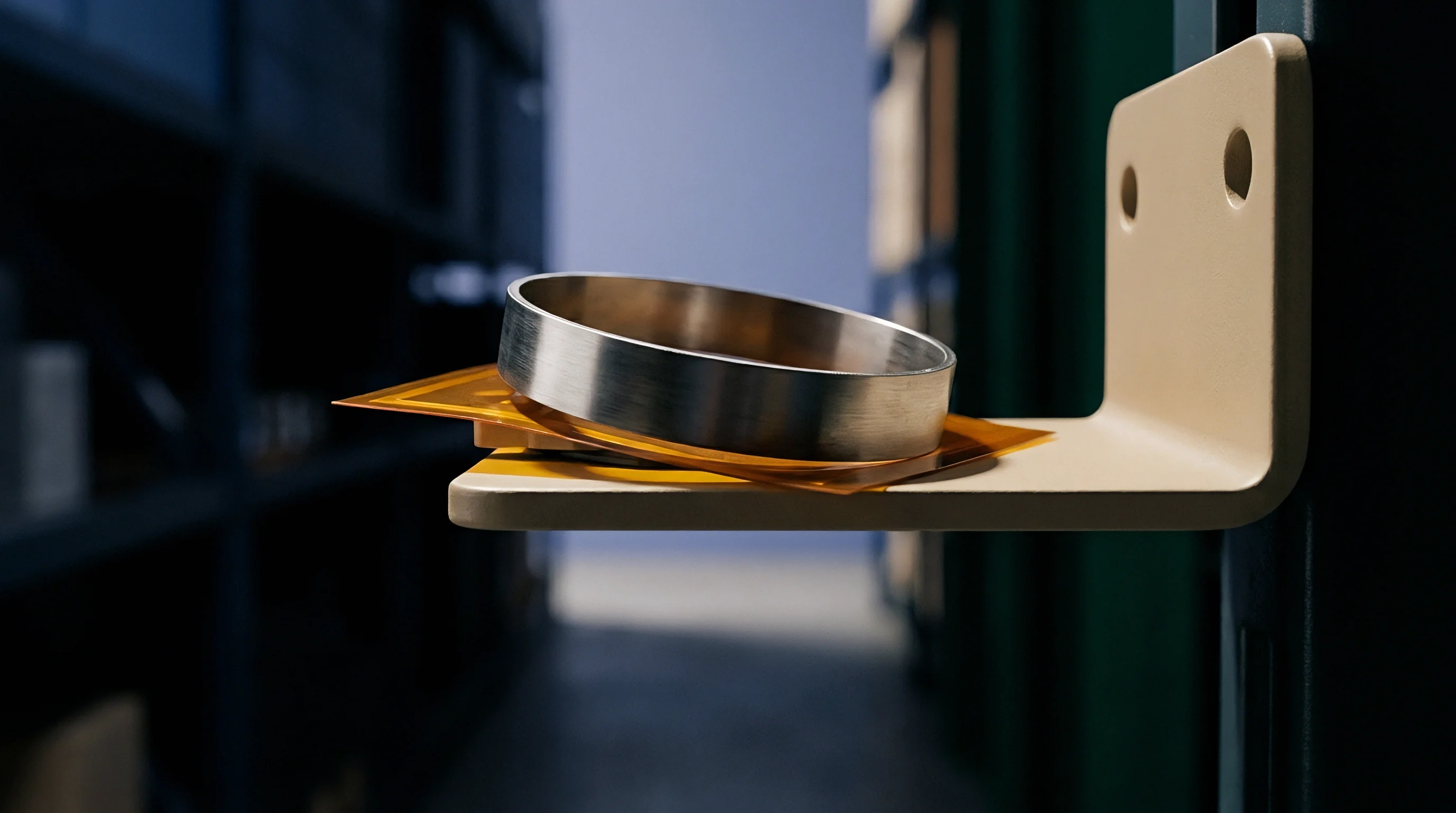
Selecting substrate materials and designing thermal boundaries dictate how external thermal fields penetrate active sensor structures. High thermal resistance substrate layers isolate sensitive die microstructures from rapid external thermal transients. However, low thermal conductivity materials slow internal heat dissipation, allowing localized steady-state thermal gradients to persist across differential sensing nodes for extended operating periods.
Alumina, glass, low-temperature co-fired ceramic, and silicon-on-insulator substrates each present distinct thermomechanical tradeoffs. Glass and fused silica offer low thermal expansion coefficients, reducing strain transfer into silicon sensing elements. Their low thermal conductivity creates persistent internal thermal imbalances under asymmetric heating, forcing system designers to balance thermal isolation against internal gradient homogenization.
| Packaging Architecture | Thermal Gradient Attenuation (dB) | Mechanical Strain Coupling (%) | Landed Unit Cost Adder (USD) | Thermal Settling Time (s) |
|---|---|---|---|---|
| Direct Die Attach (FR-4 PCB) | 0.0 | 100.0 | 0.00 | 1.2 |
| Ceramic Interposer with Soft Silicone Gel | 14.5 | 18.0 | 0.85 | 4.8 |
| Silicon-on-Isolator Suspended MEMS Island | 28.0 | 3.5 | 2.40 | 12.5 |
| Hermetic Metallic Can with Air Gap Isolators | 34.0 | 1.2 | 6.50 | 28.0 |
Package layout choices alter heat flux pathways through the sensor assembly. Placing high-dissipation components such as power regulators, line drivers, and processing cores away from differential sensor nodes prevents direct heat transfer. Symmetry in surrounding metal traces, ground planes, and copper pours balances thermal impedance, forcing heat from external sources to flow equally across both capacitive arms.
Substrate Selection Decision Rules
Sourcing and design engineering teams evaluate packaging architectures against specific operational thermal field criteria:
- Thermal Symmetry Layout requires identical metallic copper trace density and pad geometry surrounding both capacitive channels to equalize heat conduction rates.
- Strain-Relief Trenching introduces micromachined laser cuts in the substrate around the sensing region, increasing thermal resistance and blocking lateral mechanical shear forces.
- High-Conductivity Heat Spreading integrates localized copper or aluminum heat plates directly beneath the sensor die to collapse spatial thermal gradients across sensing elements.
- Decoupled Interposer Mounting separates the active sensor ceramic carrier from the main application board using compliant ball-grid arrays or flexible leads.
A supplier often claims that internal differential geometry inherently cancels all thermal effects, omitting the reality that spatial thermal gradients break geometrical symmetry under real operating conditions.


Sourcing
Procuring differential capacitive sensors with guaranteed bias stability under spatial thermal gradients requires clear qualification standards and rigorous procurement specifications. Standard manufacturer datasheets publish bias drift figures taken in isothermal environmental chambers where ambient temperature changes uniformly across the entire package. These isothermal figures conceal real-world performance failures that occur when localized thermal sources heat one side of the component on an application board.
Evaluating vendor claims demands requesting thermal gradient test dockets alongside standard qualification reports. Qualification protocols must specify non-uniform thermal stress testing, applying localized heat flux to individual package sides while recording output bias drift. Components designed without thermal symmetry considerations exhibit order-of-magnitude bias spikes during dynamic local heating events that isothermal chamber testing completely fails to expose.

Non-Uniform Thermal Qualification Testing
Testing laboratories generate controlled non-uniform thermal fields using focused infrared lasers or localized thermoelectric micro-heaters attached directly to specific package corners. The test setup monitors spatial substrate temperature distributions using calibrated thermal imaging or embedded micro-thermocouples while measuring differential capacitance output. Drift curves recorded during localized heat application reveal true mechanical and electronic gradient sensitivities.
- Mount the target sensor package on a temperature-controlled test fixture maintaining baseline ambient conditions at 298 Kelvin.
- Apply a localized thermal load using a contact heater pad attached to the left edge of the sensor substrate, delivering a constant heat flux of 50 milliwatts.
- Record real-time differential output bias voltage, common-mode capacitance, and spatial temperature delta between opposite package pins over a 300-second stabilization window.
- Repeat thermal loading on right, top, and bottom package edges to establish a comprehensive directional thermal gradient sensitivity matrix.
- Reject component batches that exceed specified bias drift limits during peak transient thermal flow conditions.
Procurement clauses written into commercial supply agreements must define explicit bias stability limits under defined spatial gradient conditions, protecting projects against unexpected board-level thermal interference.
Standard purchase contracts must stipulate that zero-point bias stability claims hold valid under spatial thermal gradients up to 0.5 Kelvin per millimeter applied across any packaging axis.
In accordance with ISO 26262 qualification standards for safety-critical sensing systems, failure modes arising from non-uniform thermal stress must be documented in formal component risk evaluations. Standard procurement agreements must mandate that suppliers notify buyers of any change to die-attach adhesive formulations, substrate ceramic suppliers, or internal lead-frame geometries. Alterations in die-attach thermal conductivity directly shift internal thermal gradient profiles, instantly invalidating original board-level calibration algorithms and expose system designs to unquantified field drift.