Spatial Thermal Gradient Mapping in Micro-Machined Silicon Accelerometer Arrays
Spatial thermal gradients across micro-machined accelerometer dies induce differential flexure expansion and zero-g bias drift remediable via symmetric layout and matrix diode compensation.

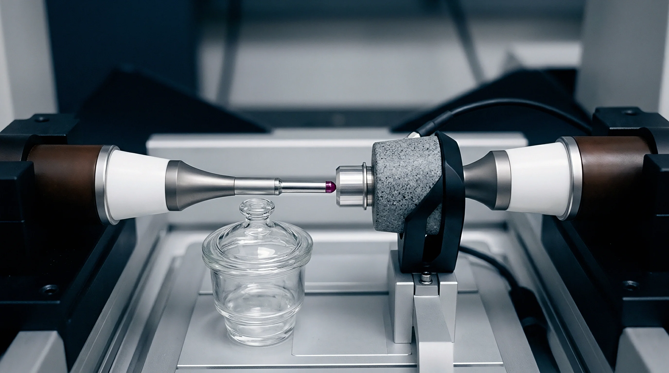
Dissipation
Energy released inside micro-systems sets up non-uniform thermal fields across microscopic substrate boundaries. When micro-machined accelerometer arrays share a silicon die with high-speed analog-to-digital converters, charge pumps, or clock generation circuitry, power distribution across the die turns asymmetrical. Heat generated by switching transistors travels through the monocrystalline silicon lattice, establishing transient and steady-state spatial temperature gradients across nearby sensing structures.
Silicon’s high thermal conductivity ~ around 148 W/(m·K) at room temperature ~ spreads heat rapidly, but microscopic heat sources still create local temperature differences of 0.1 °C to 2.5 °C over distances as small as 500 µm. In differential capacitive micro-machined accelerometers, this spatial temperature imbalance degrades mechanical bias stability, shifts zero-g offset values, and perturbs differential pickoff capacitance.
Heat moves through the substrate mainly by conduction through bulk silicon, spreading laterally before entering package structures. Local power densities within integrated application-specific integrated circuits frequently exceed 10 W/cm² across driver transistors and output amplifiers. Concentrated thermal flux causes localized lattice expansion, tilting and bowing the sensor frame.
Micro-machined accelerometer proof masses suspended by micromechanical silicon beams rely on sub-micron structural symmetry to reject common-mode mechanical noise. Thermal gradients disrupt this symmetry by altering local elastic moduli and driving differential thermal expansion along opposing beam flexures.

ASIC Energy Redistribution and Localized Temperature Fields
Integrated readout electronics convert active power into localized heat near sensor anchors. Multi-channel accelerometer arrays operating in high-bandwidth or high-dynamic-range applications draw continuous bias currents through operational transconductance amplifiers and high-rate output drivers. Power dissipation profiles across the ASIC section vary with operating modes, clock frequencies, and output load currents.
Switching events introduce dynamic thermal ripples that propagate across the interconnect interface into the MEMS structural region.
Thermal propagation speed through silicon depends on the material’s thermal diffusivity ~ its thermal conductivity divided by the product of density and specific heat capacity. Monocrystalline silicon exhibits a thermal diffusivity of roughly 88 mm²/s at 300 K. A thermal pulse generated by a switching amplifier reaches a proof mass anchor 1 mm away in about 5.7 milliseconds. Because heat spreads so quickly, dynamic operational changes within the signal conditioning ASIC instantly induce mechanical strain within sensing elements.
Thermal gradients are rarely static; variable processor workloads induce fluctuating spatial thermal profiles that show up as low-frequency bias noise in acceleration channels.
Differential capacitance pickoff circuits depend on femtofarad-level symmetry between opposing electrode pairs. When localized heating warms one capacitor electrode relative to its pair, two physical errors occur simultaneously. The change in temperature alters the local dielectric permittivity of the gas or vacuum inside the cavity while causing differential thermal expansion of the structural silicon plates.
A temperature differential of 0.2 °C across a 2 fF differential pickoff gap shifts the mechanical null position sufficiently to register a false acceleration equivalent to several milligrees.
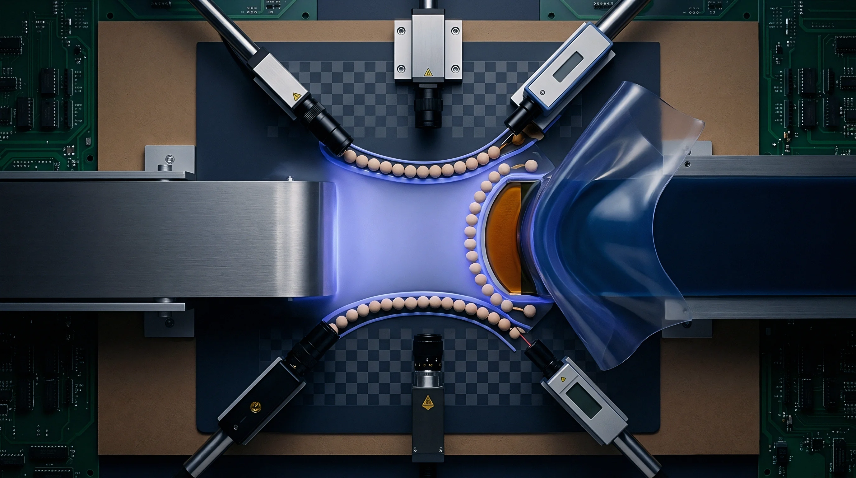
Substrate Heat Sources and Spatial Gradient Genesis
On-chip driver transistors inject non-uniform thermal power into the supporting silicon base. Trace resistance within metallic interconnect layers provides an additional source of spatially distributed thermal generation. High-current power lines running along one edge of a multi-axis accelerometer die create line heat sources that set up linear thermal gradients perpendicular to the bus geometry.
These linear gradients produce predictable thermal bending moments in the underlying silicon, though predicting the exact acceleration offset requires detailed spatial thermal mapping.
External components mounted to the printed circuit board contribute further to localized substrate gradients. Power management integrated circuits, microcontrollers, and current-sense resistors radiating thermal energy toward one side of an accelerometer package establish external thermal flux vectors. Heat flows into the package pins, through the substrate leadframe, and up through die-attach materials into the MEMS wafer.
Unequal solder joint volumes, non-uniform PCB copper plane geometry, and asymmetric routing of thermal vias force heat to enter the sensor die through non-uniform thermal impedance paths.
| Heat Source Location | Localized Power Dissipation (mW) | Substrate Distance to Proof Mass Anchor (µm) | Measured Temperature Differential (°C) | Calculated Spatial Gradient (°C/mm) | Zero-g Bias Offset Shift (mg) |
|---|---|---|---|---|---|
| Integrated Clock Generator ASIC Zone | 45.0 | 350 | 1.85 | 5.28 | 12.4 |
| Output Bus Line Transistors | 18.5 | 600 | 0.72 | 1.20 | 3.8 |
| On-Die Charge Pump Regulator | 32.0 | 450 | 1.30 | 2.89 | 8.1 |
| External PCB Power Track (Pin-Fed) | 120.0 | 1800 | 0.95 | 0.53 | 2.1 |
| Symmetric Internal Bias Reference | 4.2 | 200 | 0.08 | 0.40 | 0.3 |
Quantifying local thermal flux distribution requires examining both steady-state conditions and transient operational cycles. During cold start-up, power dissipation in the ASIC ramps up within microseconds, while the thermal capacitance of the silicon substrate delays structural equilibrium for several seconds. During this transient window, spatial gradients can peak at values up to five times higher than their steady-state equivalents.
Accelerometer arrays designed for inertial navigation or precise tilt measurement display substantial early-stage drift during thermal ramp-up. Omitting internal heat generation mechanisms from offset stability specifications leads directly to uncompensated bias drift errors on the bench.
Failing to map spatial thermal gradients during micro-machined accelerometer array design results in unresolvable mechanical offset errors, compromised tactical-grade performance targets, and costly multi-wafer mask redesign cycles.


Wafer
Monocrystalline silicon transfers heat through lattice phonon conduction with marked directional variations. Standard semiconductor manufacturing utilizes silicon wafers cut along specific crystallographic planes, typically (100) or (111) crystal orientations. Phonon scattering and thermal conduction properties along the principal crystallographic axes govern heat spreading behavior across the sensor die.
While isotropic approximations simplify preliminary thermal modeling, localized heat sources on a silicon substrate produce non-spherical thermal fronts that deform surrounding mechanical flexures along crystallographic slip planes.
Anchor points securing micro-machined proof masses to the underlying silicon substrate act as concentrated thermal conduction pathways. Because MEMS proof masses are frequently suspended over etched vacuum cavities, thermal dissipation through radiation and low-pressure gas conduction remains minimal compared to conductive transfer through physical anchor flexures. Heat flowing from the die substrate through anchor points into thin structural beams creates localized thermal gradients along the suspension flexure length.
These gradients alter the Young’s modulus of silicon locally, which decreases by approximately 50 ppm/°C near room temperature.

Anisotropic Heat Conduction and Mechanical Anchor Strain
Crystallographic orientation dictates internal thermal conduction rates along specific lattice axes. In micro-machined accelerometers with proof masses oriented along the direction of a (100) silicon wafer, thermal stress gradients couple directly into longitudinal flexural modes. Mechanical anchors positioned symmetrically around a central proof mass experience unequal thermal expansion when a spatial thermal gradient bisects the die.
This differential thermal movement shifts the mechanical reference frame of the sensor relative to its capacitive pickoff electrodes.
Mechanical stress induced by spatial thermal gradients generates piezoresistive and thermoelastic responses within structural silicon. In capacitive accelerometer arrays, mechanical stress alters the flatness of anchor points and structural frames, inducing parasitic capacitance changes unrelated to physical acceleration. In piezoresistive accelerometer arrays, thermo-mechanical stress shifts sensor element zero-point balances independently of ambient temperature changes.
Standard isotropic temperature sensors integrated onto the die edge fail to capture these localized, crystallographically driven stress concentrations.
An offset shift of 1.45 mg/°C emerges under a 0.65 °C/mm spatial thermal gradient across a 3.5 mm micro-machined silicon accelerometer die, independent of uniform ambient thermal stabilization.
Heat conduction across thin-film silicon structures differs significantly from bulk silicon thermal behavior. Micro-machined suspension beams with thickness dimensions comparable to the mean free path of phonons in silicon, which is roughly 250 to 300 nm at room temperature, exhibit reduced effective thermal conductivity due to boundary scattering. Suspension flexures measuring 1 µm in thickness display thermal conductivities up to 30 percent lower than bulk values.
This thermal conductivity reduction amplifies local thermal gradients across thin structural elements, raising temperature differentials between the proof mass and its surrounding anchor frame.

Differential Expansion across Micromechanical Suspensions
Varying temperature profiles across parallel beam flexures force unequal structural elongation. Micro-machined accelerometer arrays built with differential comb-finger structures rely on equal beam geometry to preserve structural overlap capacitance under zero acceleration. When thermal energy propagates across the array from left to right, the left suspension beam operates at a higher temperature than the right beam.
The warmer beam undergoes greater thermal expansion, displacing the entire proof mass laterally along its axis of sensitivity.
Thermal expansion mismatches also occur between silicon structural layers and oxide insulation layers. Micro-machined accelerometer fabrication processes utilize buried oxide layers in Silicon-On-Insulator substrates for structural isolation. Silicon exhibits a coefficient of thermal expansion of approximately 2.6 × 10⁻⁶ /K at 25 °C, whereas silicon dioxide exhibits a coefficient of roughly 0.5 × 10⁻⁶ /K. A spatial thermal gradient across an oxide-silicon bimorph interface induces thermal bending moments, forcing micro-machined frames to warp out of plane.
Out-of-plane structural warping alters the sense gap distance in z-axis capacitive accelerometers, changing device scale factor and sensitivity across temperature.
Substrate thermal gradients induce mechanical torque in balanced dual-proof-mass accelerometer arrays. Differential sensing architectures utilize counter-moving proof masses to reject external vibration and common-mode mechanical shocks. When localized thermal gradients alter the stiffness of the flexures supporting one proof mass without affecting the second mass identically, common-mode rejection collapses.
The differential signal processing channel interprets the resulting asymmetric structural deflection as a valid physical acceleration vector, introducing dynamic zero-g bias offsets into high-precision measurements.
Standard low-stress oxide layers and global die temperature calibration are often presumed to eliminate thermal drift, yet localized sub-millimeter thermal gradients still induce mechanical distortion.


Calorimetry
Measuring internal temperature distributions across microscopic sensing arrays requires localized transducer networks. Traditional thermometry relying on a single off-chip thermistor or a single integrated junction diode provides only a zero-dimensional average die temperature. This aggregate measurement completely misses directional temperature differences across the sensor face.
Spatial thermal gradient mapping demands dense networks of microscopic temperature sensors distributed strategically across the active micro-machined silicon geometry to capture two-dimensional thermal vector fields in real time.
Calorimetric mapping techniques evaluate spatial thermal profiles through both contact electrical methods and non-contact optical diagnostics. Contact methods integrate micro-diode matrices or thermopile structures directly into structural silicon frames during wafer processing. Non-contact methods utilize infrared thermography microscopy or micro-Raman spectroscopy during bench testing to validate spatial thermal models under full electrical operational loads.
Reconciling micro-Raman optical thermal measurements with integrated diode electrical readings provides the foundation for accurate thermal gradient compensation matrices.

Integrated Semiconductor Diode Sensing Networks
Forward voltage drops across p-n junctions provide predictable voltage shifts of two millivolts per kelvin. Placing array networks of microscopic p-n junction diodes across the MEMS perimeter and adjacent ASIC regions enables real-time temperature sensing at specific micro-structural coordinates. Sensing diode cells designed with ultra-small footprints, such as 20 µm by 20 µm, introduce minimal parasitic capacitance into signal lines while providing rapid thermal response times under 500 microseconds.
Differential diode pairs positioned on opposing sides of a MEMS proof mass anchor form direct spatial thermal gradient detectors. Biasing two identical p-n junctions with matching constant-current sources yields a differential output voltage directly proportional to the localized spatial temperature difference across the inter-diode span. Connecting these differential voltage outputs directly to low-noise delta-sigma analog-to-digital converters allows the system to read spatial thermal gradients down to 0.01 °C resolution, enabling dynamic firmware-based gradient compensation.
Thermopile structures fabricated using alternating polysilicon and metal interconnect traces leverage the Seebeck effect to generate direct voltage outputs without continuous forward current biasing. Integrated micro-thermopiles routed across isolation trenches measure localized heat flux directly. Thermopiles output zero voltage when temperature balance exists across their junctions, eliminating zero-point offset errors inherent to active diode sensing circuits.
However, thermopile integration requires additional silicon surface area and process masks, increasing wafer-level manufacturing costs.

Infrared Micro-Thermography and Optical Mapping
Radiative emission profiling across polished silicon die surfaces yields high-resolution surface maps. Standard infrared cameras lack the spatial resolution required to resolve sub-micron thermal gradients across micro-machined suspension flexures. Micro-IR thermography optical systems equipped with specialized microscope objectives achieve spatial resolutions down to 2.5 µm per pixel.
Calibrating thermal emissivity across non-uniform silicon, aluminum, and oxide surfaces requires applying thin, uniform matte carbon coatings or executing precise multi-temperature radiometric surface emissivity calibrations before data collection.
Micro-Raman spectroscopy determines local silicon structural temperature by measuring inelastic laser light scattering shifts. The Raman peak frequency of monocrystalline silicon shifts predictably toward lower wavenumbers as local temperature increases due to lattice thermal expansion and anharmonic phonon interactions. Focusing a 532 nm laser excitation beam through a high-numerical-aperture optical microscope enables spatial thermal mapping with sub-micron lateral resolution and a temperature accuracy of ±0.5 °C. Micro-Raman mapping operates through transparent encapsulation windows, enabling non-destructive thermal profiling inside hermetically sealed MEMS cavity packages.
| Mapping Methodology | Spatial Resolution (µm) | Temperature Resolution (°C) | Measurement Bandwidth (Hz) | Non-Invasive Qualification Rank | Wafer Test Overhead |
|---|---|---|---|---|---|
| Integrated Diode Matrix Networks | 15 to 50 | 0.01 | 2000 | Fully Integrated | Low (Built-in Circuitry) |
| Micro-Raman Spectroscopy | 0.5 to 1.0 | 0.50 | 10 | Non-Contact Optical | High (Specialized Optics) |
| Micro-IR Thermography | 2.5 to 10.0 | 0.10 | 60 | Non-Contact Optical | Medium (Coating Required) |
| Integrated Polysilicon Thermopiles | 20 to 100 | 0.005 | 5000 | Fully Integrated | Medium (Extra Mask Layers) |
| Liquid Crystal Thermography | 5.0 to 15.0 | 0.20 | 2 | Surface Applied | High (Destructive Coating) |

Why Do Dynamic Gradients Outpace Single-Point Compensation?
Single sensor nodes measure local absolute temperature while failing to detect directional thermal vector shifts. When a high-power transient occurs on an adjacent circuit module, heat propagates across the sensor substrate as a moving thermal wave front. The local temperature at a single-point sensor located on the far edge of the die remains unchanged while the wavefront passes directly across the central MEMS proof mass structure.
Consequently, single-point compensation algorithms apply incorrect calibration coefficients, compounding mechanical acceleration errors during dynamic thermal transients.
Dynamic spatial thermal gradients establish internal mechanical forces that scale with the spatial derivative of the temperature field rather than absolute temperature magnitude. Micro-machined beam flexures subject to non-linear thermal profiles experience complex structural bending modes that cannot be modeled as simple scalar functions of average die temperature. Mapping spatial temperature vectors across multi-diode arrays provides the higher-order mathematical inputs required to compute true instantaneous mechanical deformation vectors.
Applying standard single-point thermal compensation calibration models under IEEE 1451 smart transducer specifications fails to satisfy performance requirements when spatial thermal gradients exceed 0.1 °C/mm across the sensor substrate.
Standard qualification procedures defined in AEC-Q103-002 section 4.3 require verifying structural sensor performance across uniform thermal soak conditions, explicitly leaving unaddressed the zero-g bias offsets induced by transient spatial thermal gradients across multi-chip modules.


Layout
Structural symmetry across micro-machined proof mass geometries minimizes offset shifts induced by localized heat inputs. Designing MEMS sensor arrays for high thermal gradient rejection requires arranging mechanical flexures, anchors, and capacitive pickoff comb structures along natural isothermal contours. When structural components sit along identical temperature contours, thermal expansion occurs uniformly across all functional sides, preserving mechanical null alignment under high localized heat flux.
Thermal isolation barriers integrated directly into the silicon substrate interrupt direct heat conduction paths between active ASIC circuitry and sensitive micro-machined mechanical elements. Etched deep reactive ion etching trenches filled with low-conductivity materials or sealed under high vacuum create high-impedance thermal boundaries. By forcing heat flux to flow around sensitive proof mass anchors, thermal isolation structures flatten spatial thermal gradients across the active sensing zone.

Thermal Isotherms and Symmetrical Structural Geometries
Aligning mechanical flexures along constant temperature contours eliminates differential expansion across pickoff electrodes. Quad-pole accelerometer array layouts place four distinct sensing cells in a symmetrical cross configuration around a central axis. Connecting these four sensing cells in a cross-differential electrical configuration cancels linear spatial thermal gradients across both principal die axes.
Linear thermal gradients affect opposing sensing cells equally and oppositely, allowing differential signal processing channels to reject spatial thermal noise while preserving true mechanical acceleration signals.
Center-anchor proof mass topologies provide superior thermal gradient rejection compared to corner-anchored frame designs. A single central anchor point grounds the micro-machined proof mass to the substrate at one location, allowing the outer frame to expand isotropically outward during thermal transients. Corner-anchored frames constrain structural expansion at multiple distant points across the substrate, translating local substrate thermal gradients into severe internal compressive or tensile mechanical stresses that alter suspension flexure spring constants.
Designing micro-machined accelerometer arrays with central anchor topologies and quad-symmetric pickoff configurations rejects linear spatial thermal gradients completely while suppressing higher-order non-linear gradients by over 20 dB.
Symmetric placement of localized dummy heat sources balances internal thermal fields across silicon dies. Integrating low-power polysilicon heating elements along cold die edges allows active thermal management systems to mirror the power dissipation profiles of adjacent ASIC drivers. When an active circuit block dissipates 20 mW on the left edge of the die, the control system energizes the corresponding dummy heater on the right edge, forcing spatial temperature gradients to remain symmetrical across the central MEMS sensing axis.

Etched Isolation Cavities and Vacuum Boundaries
Deep reactive ion etching forms physical air gaps that block conductive heat transport between adjacent circuit modules. Etching full-depth silicon isolation trenches around the perimeter of the mechanical sensing area increases conductive thermal resistance by multiple orders of magnitude. Heat generated within the read-out electronics section must travel around the perimeter isolation channels, extending the thermal path length and dissipating energy into the package substrate before reaching sensor anchors.
Vacuum encapsulation structures reduce convective heat transfer across micro-machined cavities. High-g and high-precision capacitive accelerometers rely on vacuum hermetic sealing to achieve targeted quality factors and reduce thermoelastic damping noise. Vacuum encapsulation eliminates internal gas-phase thermal convection and conduction between the lid cap and the proof mass, restricting heat transport exclusively to solid-state conduction through silicon anchor flexures.
Structural failure modes stemming from severe spatial thermal gradients across silicon MEMS arrays follow clear mechanical and electrical patterns:
- Thermo-Mechanical Anchor Shear occurs when localized substrate expansion forces structural anchors out of alignment, introducing permanent zero-g offset shifts into capacitive sensor channels.
- Differential Comb Finger Shorting manifests when asymmetric thermal expansion forces inter-digitated capacitive electrodes into physical contact, causing signal rail saturation.
- Buckling Instability in Suspension Flexures develops when localized thermal compressive stress exceeds the Euler buckling threshold of thin silicon beams, degrading structural mechanical stability.
- Resonant Frequency Splitting happens when spatial thermal gradients alter the spring constants of dual orthogonal flexures unequally, splitting degenerate resonant modes and inducing axis cross-talk.
- Asymmetric Thermoelastic Damping emerges when thermal gradient fields alter internal energy dissipation rates across structural flexures, altering local mechanical quality factors.
Layout geometry must prioritize thermal symmetry over silicon die area conservation whenever tactical-grade bias stability is required under variable thermal conditions.


Packaging
Encapsulation materials introduce mismatched thermal expansion behavior around the enclosed micro-system. Over-molded plastic packages, ceramic cavity housings, and metallic quad-flat no-lead packages exhibit thermal expansion coefficients ranging from 4 ppm/K to over 16 ppm/K, whereas silicon operates near 2.6 ppm/K. When external temperatures fluctuate or internal circuits dissipate power, non-uniform package expansion transfers severe thermo-mechanical stresses into the underlying silicon substrate, distorting the spatial thermal mapping profile of the internal accelerometer array.
Die-attach adhesives present a primary source of localized thermal gradient anomalies across micro-machined accelerometer dies. Silver-filled epoxy materials and eutectic solder preforms establish the mechanical and thermal bond between the silicon substrate and the package leadframe. Non-uniform adhesive thickness, void formation within epoxy layers, and localized delamination create localized thermal impedance variations beneath the die.
Heat flowing downward toward the external heat sink encounters non-uniform thermal resistance, transforming uniform downward flux into severe spatial thermal gradients across the active MEMS plane.
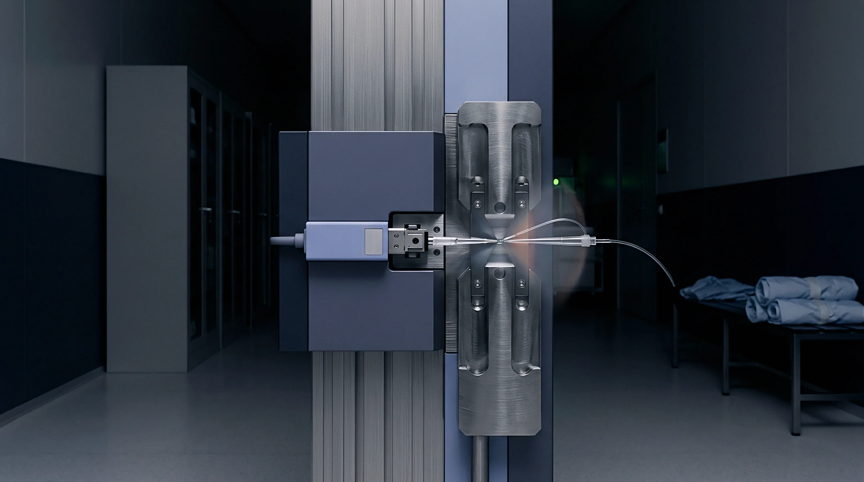
Die Attach Delamination and Contact Thermal Resistance
Adhesives coverage gaps beneath the substrate interrupt uniform downward heat conduction. Voiding ratios exceeding 5 percent in structural die-attach layers induce micro-scale hot spots directly above the void boundaries. Heat generated by on-chip sources accumulates above air-filled void pockets due to the low thermal conductivity of trapped gas, which is roughly 0.026 W/(m·K), establishing localized thermal gradients up to 4 °C/mm across the silicon base.
Eutectic gold-silicon solder bonding provides significantly higher thermal conductivity than conductive epoxies, reaching approximately 295 W/(m·K). However, the high processing temperatures required for eutectic bonding generate elevated residual mechanical strain within the silicon substrate upon cooling. Spatial variation in eutectic alloy crystallization induces localized stress fields that interact with spatial thermal gradients, exacerbating zero-g bias drift during operational thermal cycling.
| Packaging Layer Material | Bulk Thermal Conductivity (W/m·K) | Coefficient of Thermal Expansion (ppm/K) | Typical Layer Thickness (µm) | Interfacial Thermal Resistance (K·mm²/W) | Observed Spatial Gradient Contribution |
|---|---|---|---|---|---|
| Monocrystalline Silicon Substrate | 148.0 | 2.6 | 350 | Negligible (Bulk) | Base Conductive Layer |
| Silver-Filled Epoxy Die Attach | 1.8 to 2.5 | 35.0 to 50.0 | 25 | 12.5 to 25.0 | High (Void Sensitive) |
| Eutectic Au-Si Solder Preform | 295.0 | 14.2 | 15 | 1.2 to 2.5 | Low (High Stress) |
| Alumina Ceramic Package Base | 24.0 to 30.0 | 6.5 to 7.2 | 1000 | 3.5 to 6.0 | Moderate (Stable) |
| Epoxy Mold Compound (Encapsulated) | 0.8 to 1.2 | 10.0 to 16.0 | 1500 | 18.0 to 35.0 | High (Asymmetric Flux) |

System Boundary Conditions and Outer Enclosure Flux
External chassis heating creates sweeping spatial temperature fields across multi-chip modules. Accelerometers integrated into industrial automation systems, automotive powertrains, or aerospace avionics experience severe ambient thermal radiation and conductive heat transfer through mounting screws. Asymmetric mechanical attachment of the sensor package to the host circuit board creates preferential conductive heat paths, forcing external thermal energy to enter through specific package pins.
Audit and qualification of spatial thermal integrity across packaged micro-machined accelerometer arrays require rigorous bench evaluation using standard procedures:
- Mount the packaged accelerometer array onto a temperature-controlled copper cold plate within a vacuum calibration chamber operating below 10⁻⁴ Torr.
- Connect integrated p-n junction diode sensing networks to high-resolution digital multimeters to establish baseline isothermal zero-voltage calibration points at 25 °C.
- Apply a calibrated step-function power load to internal ASIC driver circuits while monitoring spatial temperature distributions across all embedded diode sensing nodes simultaneously.
- Record zero-g bias offset outputs across all accelerometer channels at 100 Hz sampling rates during the initial 60-second transient thermal equalization window.
- Map spatial thermal gradient vectors by computing localized spatial derivatives between adjacent diode node readings across the die surface.
- Correlate instantaneous spatial thermal gradient magnitudes against measured acceleration offset shifts to extract spatial thermal sensitivity coefficients for each array axis.
- Inspect die-attach interface integrity using acoustic microscopy to confirm that identified spatial thermal hot spots align with structural adhesive voiding locations.
Interfacial thermal voids within silver-filled epoxy die-attach layers induce localized thermal gradients exceeding 3.8 °C/mm across substrate surfaces, increasing zero-g bias instability by a factor of four.
How do advanced organic substrate materials and low-stress silicone die-attach formulations mitigate spatial thermal gradient generation across tactical-grade inertial measurement units exposed to extreme environmental ramp rates?


Mitigation
Correction strategies for spatially non-uniform thermal fields leverage both physical decoupling and digital matrix operations. Eliminating spatial thermal gradient errors in micro-machined accelerometer arrays requires an integrated approach combining balanced wafer layout design, optimized package die-attach processing, and real-time firmware signal processing. While physical layout rules minimize gradient formation, residual thermal vectors demand dynamic algorithmic correction to achieve sub-milligee bias stability across industrial and tactical environments.
Real-time firmware mitigation maps instantaneous output signals from distributed thermal diode matrices into high-order polynomial compensation algorithms. Rather than relying on scalar temperature lookup tables, modern signal conditioning ASICs execute full spatial thermal matrix calculations. Inputting multiple discrete temperature readings enables the processor to calculate both absolute average die temperature and directional thermal gradient vectors across orthogonal axes, dynamically subtracting thermal-gradient-induced acceleration offsets before outputting data to host system buses.

Real Time Matrix Calibration and Array Processing
Embedded digital signal processors execute multi-variable polynomial equations to offset gradient errors. The mathematical model for zero-g bias correction represents acceleration offset as a multi-variable function containing both absolute temperature terms and spatial temperature gradient terms. Evaluating temperature differences between opposing die corners yields spatial gradient inputs across the length and width of the sensor substrate.
Calibrating multi-variable spatial thermal models requires multi-point thermal chamber testing during sensor manufacturing. Sweeping ambient chamber temperatures while simultaneously toggling internal ASIC power modes populates calibration matrices with explicit gradient sensitivity coefficients. Standard calibration routines store these coefficients in non-volatile memory embedded within sensor modules.
During operational deployment, the signal conditioning ASIC samples integrated diode arrays every millisecond, continuously updating thermal gradient compensation vectors.
Evaluating multi-axis accelerometer arrays for thermal robustness requires a structured decision checklist before committing designs to commercial production:
- Thermal Isothermal Mapping Verification confirms whether all micromechanical suspension flexures align perfectly along predicted constant temperature contours under maximum ASIC power dissipation.
- Die Attach Interface Integrity Standard enforces less than 2 percent total adhesive voiding under the MEMS die, with zero individual voids exceeding 100 µm in diameter.
- Distributed Thermal Sensor Coverage verifies that integrated p-n junction sensing nodes monitor all critical anchor flexures and major internal power dissipation sources across the die.
- Common Mode Rejection Ratio Audit evaluates whether differential capacitive pickoff circuits reject linear spatial thermal gradients up to 5.0 °C/mm without exceeding specified zero-g offset limits.
- Dynamic Transient Compensation Stability checks that real-time firmware algorithms maintain offset stability during thermal ramp rates exceeding 10 °C per minute.

Active on Chip Thermal Equalization Devices
Integrated polysilicon resistors dissipate targeted thermal power to cancel internal temperature asymmetry. Active thermal management systems deploy micro-heaters positioned symmetrically across silicon substrates. When internal diode sensing matrices detect an unexpected thermal gradient caused by external heat sources or ASIC workload shifts, control loops energize specific micro-heaters to re-establish spatial thermal equilibrium across the sensor frame.
Closed-loop thermal balancing circuits utilize pulse-width modulation to drive low-impedance polysilicon heating elements. Adjusting duty cycles based on real-time differential temperature feedback flattens spatial temperature profiles to within 0.05 °C across the entire active MEMS area. Active thermal management consumes additional operating power, typically 5 to 25 mW depending on environmental thermal gradient severity, making it suitable for applications prioritizing absolute bias stability over low-power operation.
Implementing active thermal management requires precise control bandwidth tuning. Thermal time constants associated with substrate heat conduction dictate the maximum bandwidth of closed-loop heater feedback channels. If the heater control loop bandwidth exceeds the thermal diffusion frequency of the silicon substrate, thermal oscillations develop, introducing artificial periodic bias noise into acceleration output channels.
Tuning control loop response times to remain safely below structural thermal cutoff frequencies prevents instability while suppressing ambient low-frequency thermal transients.
Combining passive wafer symmetry, vacuum cavity thermal isolation, structural die-attach void minimization, and real-time spatial matrix compensation allows micro-machined accelerometer arrays to maintain sub-milligee zero-g bias stability under severe dynamic thermal conditions.