Cascade Enable Daisy Chaining for High Density Sensor Arrays
Cascade enable daisy chaining reduces host controller interface traces to four lines while dynamic address framing scales high-density sensor arrays efficiently.


Pin
High-density sensor grids installed across tight mechanical enclosures run into serious routing bottlenecks under standard microcontroller pin layouts. Connecting sixty-four pressure or thermal sensors with dedicated chip-select lines means running sixty-four individual traces across the board. That fan-out quickly saturates signal layers, forces the use of complex microvia stackups, and drives up fabrication costs.
Standard serial peripheral interfaces and inter-integrated circuit buses lack the pin-count efficiency needed when high spatial resolution demands packed component spacing.
A cascade enable architecture cuts through trace congestion by replacing separate select lines with a pass-through enable signal passed from node to node. Each sensor integrated circuit in the array incorporates a dedicated input pin for cascade enable alongside a dedicated output pin for downstream propagation. Array nodes connect in a physical daisy chain where the host controller manages only the first enable input in the sequence.
The remaining devices pass activation tokens down the chain as address assignment completes, maintaining a fixed interface footprint regardless of total sensor count, though package geometry ultimately dictates the routing layout.

Hardware Addressing Limits in Dense Sensor Footprints
Integrating sub-millimeter land grid array packages onto flexible substrates exposes the physical limits of trace fan-out. A standard twelve-terminal land grid array measuring two millimeters by two millimeters with a half-millimeter terminal pitch leaves minimal copper clearance between surface pads. Routing distinct select lines out of an eight-by-eight matrix formatted in this package footprint requires an eight-layer printed circuit board stackup using buried microvias; trace resistance drops signal amplitude, while dense parallel runs increase capacitive coupling and induce crosstalk during high-speed serial transfers.
Digital multiplexers positioned at array perimeters can trim trace counts arriving at the host controller. Multiplexer integration adds active components, consumes perimeter board real estate, and introduces signal propagation delays across the select matrix. The additional integrated circuits elevate total assembly failure points while failing to solve routing congestion within the interior footprint of the sensor matrix.
Direct daisy-chain pass-through wiring eliminates peripheral multiplexers entirely, collapsing select line requirements to a single digital control output from the primary processor.

Pass-Through Enable Hardware Architecture
The internal switch architecture of a cascade-enabled sensor IC isolates the local serial bus receiver until the upstream enable line signals active state. Internal pull-down resistors hold the enable input low during initial power application. While the enable input sits below the logic low threshold, the device maintains its serial interface pins in a high-impedance state, ignoring all clock and data traffic on the shared bus lines.
This high-impedance isolation prevents bus contention when multiple unconfigured sensors reside at identical default bus addresses.
| Parameter Symbol | Parameter Description | Min Value | Max Value | Unit |
|---|---|---|---|---|
| V_IL_CE | Cascade Enable Input Low Voltage | -0.3 | 0.3 x V_DD | V |
| V_IH_CE | Cascade Enable Input High Voltage | 0.7 x V_DD | V_DD + 0.3 | V |
| t_PROP_CE | Enable Pass-Through Propagation Delay | 8.5 | 22.0 | ns |
| I_LEAK_CE | Enable Pin Input Leakage Current | -1.0 | 1.0 | µA |
| C_IN_CE | Enable Input Terminal Capacitance | 2.1 | 4.5 | pF |
Applying a logic-high state to the first enable input wakes the initial sensor in the chain. The host controller executes address assignment over the shared serial bus, reconfiguring the active sensor from its default address to a unique network address. Once address confirmation registers in the internal control state machine, the sensor asserts logic high on its downstream enable output pin.
This output transition connects directly to the enable input of the second sensor, waking it for sequential address configuration while the first sensor transitions to normal measurement operational mode.
Routing individual select traces across high-density sensor grids escalates printed circuit board layer counts and multiplies trace crossover noise.
Designing a high-density matrix with discrete chip-select traces across sixty-four nodes forces printed circuit board stackups from four layers to eight layers, inflating raw fabrication expenditure before component assembly begins.

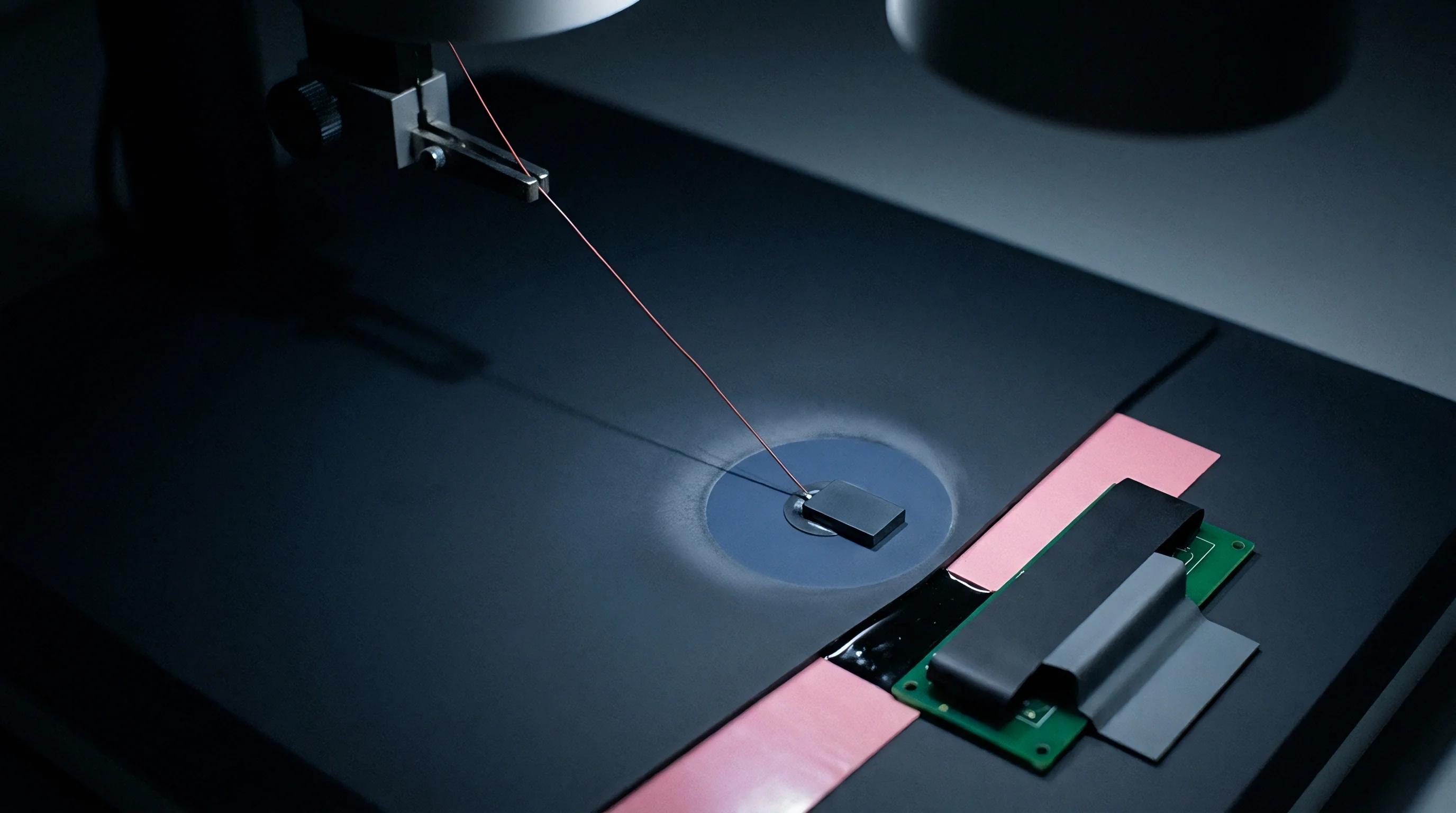
Framing
Power-on state initialization across an unenumerated serial array requires a deterministic sequence to prevent address contention on shared communication lines. When main system power stabilizes, every sensor in the array resets its internal command registers to factory default conditions. Without physical isolation or dynamic enable gating, issuing a bus command causes every integrated circuit to respond simultaneously, pulling data lines low and generating bus collisions.
Cascade enable framing establishes a hardware-enforced sequence where only one device presents an active address to the bus at any point during initialization.
The initialization frame opens when the host processor asserts the master enable line connected to device zero. The active device captures the subsequent serial frame, recognizing its factory default address. The host writes a new software-defined device address into volatile configuration memory, shifting the internal control logic out of configuration mode.
The internal switch then drives the downstream enable line to system voltage, passing execution authority to the adjacent node without host register polling overhead.

Sequential Enumeration Register State Machines
Internal state machine design dictates how quickly an array transitions from reset to operational readiness. The state machine evaluates the status of the cascade enable input pin at every system clock edge. Transition from sleep mode to configuration mode requires the enable pin to hold logic high for a minimum setup time before the first serial clock edge arrives, preventing address collisions from pulling down the bus.
- Power application initializes internal reset timers and forces all downstream cascade enable outputs to logic low.
- Host processor asserts logic high on the primary cascade enable control trace connected to array index zero.
- Array index zero detects the high state, wakes internal clock oscillators, and opens its serial bus receiver at default address 0x68.
- Host transmits a configuration payload containing the targeted unique network address for index zero.
- Index zero commits the network address to internal registers and asserts logic high on its downstream enable output pin.
- Array index one senses logic high on its enable input, opens its bus receiver at default address 0x68, and awaits the next configuration frame.
- Host repeats single-address writes until the final node in the array confirms configuration and raises the terminal status flag.
Serial peripheral interface configurations utilize a similar state progression using shift register mechanics. In cascaded serial peripheral interface topologies, data passes sequentially through internal register chains. The framing window stays open while the enable signal remains low, latching command bytes into internal memory arrays only when the enable transition returns high at frame closure.

What Limits Daisy Chain Length across Printed Circuit Arrays?
Cumulative propagation delay across pass-through enable logic paths imposes hard limits on maximum array node counts. Each sensor internal logic gate introduces a propagation delay ranging from eight to twenty-two nanoseconds between its enable input pin and downstream output pin. In a chain containing one hundred twenty-eight sensors, cumulative hardware delay on the enable signal line reaches nearly three microseconds from head to tail.
| Interface Topology | Host I/O Lines | Max Nodes | Address Overhead | Enumeration Speed |
|---|---|---|---|---|
| Discrete SPI CS | N + 3 | Limited by pins | Zero | Fastest |
| Cascade Enable I2C | 3 | 127 | 1 Byte/Node | Moderate |
| SPI Daisy Chain | 4 | Unbounded | Bit-shift Shift | Slow for deep chains |
| Shared I2C Demux | Log2(N) + 2 | 64 | Demux switching | Moderate |
Bus capacitance presents an additional physical boundary. Shared data and clock lines trace across every sensor terminal in the array. Each input terminal contributes between two and five picofarads of parasitic capacitance to the printed trace, alongside substrate capacitance from polyimide flex boards.
A sixty-four node array frequently presents total bus capacitance exceeding three hundred picofarads. High capacitance distorts clock edge rise times, requiring lower bus frequency operation to maintain timing margins unless active bus pullup accelerators sit along the trace.
A 400 kilohertz serial clock frequency limits maximum daisy chain enumeration time to 1.2 milliseconds per sensor node under nominal supply voltage.
Unresolvable address collisions during startup often track back to internal reset logic state hazards rather than power rail rise-time instability.

Routing
Physical interconnect layout on ultra-thin polyimide substrates demands strict control over line resistance and parasitic capacitance. Flexible printed circuit arrays deployed in tactile sensing or structural health monitoring applications endure continuous mechanical flexing. Differential flexing shifts trace geometries, altering line impedance and risking micro-fractures in copper traces.
Route optimization balances signal integrity against mechanical fatigue limits across long daisy-chain configurations.
Designing the physical path for pass-through enable signals requires localized point-to-point connections between adjacent sensors rather than long continuous traces back to a central host. The cascade enable output of sensor node N connects directly to the enable input of sensor node N+1 using short surface layer traces. This localized routing structure keeps enable signal trace lengths under two millimeters on 0.5 millimeter pitch footprints, reducing parasitic inductance and eliminating signal reflection risks without requiring termination resistors.

Parasitic Capacitance and Signal Integrity on Extended Flex Substrates
Polyimide flex substrates exhibit higher dielectric losses and parasitic capacitance than standard FR4 glass-epoxy materials. Substrate thickness of twenty-five micrometers yields trace-to-ground capacitance up to thirty picofarads per meter for standard three-mil trace widths. Parasitic capacitance degrades serial clock edge sharp transitions, changing square waves into exponential charging curves that confuse internal Schmidt triggers inside sensor interface receivers.
Series damping resistors placed near serial clock and data transmission source pins suppress overshoot ringing caused by long line inductance. A resistance value of thirty-three ohms inline with data output terminals dampens high-frequency reflections on arrays extending past fifty centimeters, where flex cables add parasitic trace inductance. Power distribution routing alongside signal traces demands low-resistance copper pouring to prevent voltage drops from starving downstream array nodes during concurrent sensor measurement cycles.
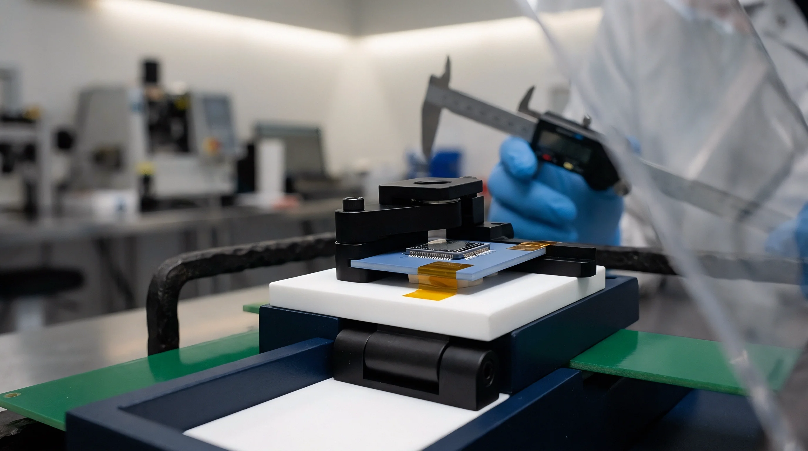
Land Pattern and Stencil Optimization for Sub-Millimeter Packages
Land pattern design for small bottom-terminated packages dictates production assembly yields. Land grid array packages with twelve terminals on a half-millimeter pitch require precise copper pad dimensions to prevent solder bridging between adjacent cascade enable inputs and main supply rails. Solder mask defined pads restrict solder flow, maintaining high dimensional stability across reflow cycles.
Pad dimensions extending zero point zero five millimeters beyond package perimeter boundaries allow reliable automated optical inspection joint verification.
- Bridging Short Circuits occur between adjacent cascade enable terminals when stencil aperture area ratios drop below zero point six six.
- Open Terminal Defects develop on interior package pads when solder paste volume shrinks below nominal thickness tolerances.
- Void Formation Incursion inside ground thermal pads elevates thermal resistance and destabilizes internal reference voltage logic circuits.
- Substrate Layer Delamination arises during reflow exposure if polyimide materials retain moisture above IPC Class 3 limits.
- Component Tombstoning Crises manifest during reflow when uneven surface tension affects asymmetric terminal layout geometry.
Reflow profile drift quickly ruins joint integrity. Stencil aperture design requires a ten percent area reduction relative to copper pad size, utilizing electro-polished nickel stencils of one hundred micrometer thickness to ensure clean paste release during high-speed automated placement.
Solder paste volume reduction on sub-millimeter package pads prevents bridging between adjacent pass-through enable traces.
Widening land pattern copper dimensions beyond vendor specifications destabilizes surface tension during reflow, pulling sub-millimeter packages off center and creating open circuits on interior enable terminals.

Timing
Signal propagation down a serial cascade line accumulates setup delays that restrict maximum operational clock frequencies. Every logic inverter, switch gate, and internal level translator within a sensor enable path contributes propagation delay. As the logic transition ripples down the chain, downstream sensors experience delayed enablement relative to host command transmission.
System timing budgets accommodate cumulative enable delays to prevent host software from issuing configuration commands to unready sensor nodes.
Reset setup time requirements dictate the hold duration of the master enable line prior to initiating bus communication. Sensor integrated circuits require a stabilization window following enable signal assertion to power up internal analog front-ends and settle voltage reference nodes. Attempting to execute serial transactions during this stabilization window generates corrupt data reads or drops configuration byte writes completely.

Propagation Accumulation and Clock Skew Bounds
Internal propagation delay tPROP:CE scales linearly with total chain length. Clock signal lines, routed in parallel to all array nodes, present near-simultaneous clock edges to every sensor receiver. The enable signal, propagating sequentially through internal logic switches, arrives out of phase with clock timing on downstream nodes.
This phase mismatch creates clock skew hazards where a downstream sensor receives serial clock pulses before its enable input fully crosses the logic high input threshold voltage VIH.
Clock jitter degrades sample phase alignment. System designers cap maximum cascade length by calculating the point where cumulative propagation delay equals half the serial clock period. At a four hundred kilohertz clock frequency, the half-period window equals one thousand two hundred fifty nanoseconds.
Assuming a worst-case per-node propagation delay of twenty-two nanoseconds, cumulative enable delay reaches the half-period limit at fifty-six nodes, requiring frequency derating for larger matrix dimensions.

Worked Enumeration Latency Calculation for a 64-Node Sensor Array
Consider a tactile sensing matrix comprising sixty-four pressure sensors linked via a cascade enable inter-integrated circuit bus running at standard four hundred kilohertz clock speed. The host processor executes an initialization sequence to assign unique network addresses from 0x10 to 0x4F. The system operates from a three point three volt supply, and datasheet specs define per-node parameters as follows:
Base parameter values assigned for latency modeling:
- Enable propagation delay tPROP:CE = 15,ns per node
- Internal stabilization delay tSTAB = 50,μs per node
- Bus command byte sequence NBYTES = 3,bytes per address write sequence
- Bits per byte transaction NBITS = 9,bits including clock acknowledge bit
Calculating single-node configuration latency tNODE requires summing bit transmission time, stabilization delay, and physical enable propagation delay:
Bit Duration tBIT = frac1400,kHz = 2.5,μs Transmission Time tTX = 3 × 9 × 2.5,μs = 67.5,μs tNODE = tTX + tSTAB + tPROP:CE = 67.5,μs + 50,μs + 0.015,μs = 117.515,μs
Total enumeration time TTOTAL for the complete sixty-four node array sums single-node latency across all sixty-four positions plus cumulative enable propagation delay across the length of the string:
TTOTAL = sumk=164 tNODE(k) = 64 × (67.5,μs + 50,μs) + sumk=164 (k × 15,ns) TTOTAL = 7520,μs + 15,ns × frac64 × 652 = 7520,μs + 31.2,μs = 7.5512,ms
The mathematical evaluation shows that internal analog front-end stabilization time (50,μs) dominates total enumeration latency, while propagation delay across pass-through enable gates (31.2,μs) accounts for less than one percent of total startup overhead.
Standard IPC A 610 Class 3 acceptance criteria mandate zero solder bridging across 0.4 millimeter pitch terminal arrays subjected to thermal cycling.
Whether dynamic edge-triggering logic on downstream enable pins can eliminate cumulative propagation delays across extended two-hundred-node sensor strings remains an open question for silicon designers.


Recovery
Hardware failures inside a linear daisy chain isolate every downstream sensor node from the main host controller. An open solder joint on an enable pass-through terminal halts array configuration at the failure point. Solder joint fatigue under repeated mechanical strain breaks physical contact, leaving downstream nodes permanently unenabled in high-impedance state.
Diagnostic logic inside host firmware detects these configuration halts, isolating fault locations by querying address completion flags.
Fault recovery strategies implement secondary routing paths or bi-directional enable pass-through lines. Bi-directional enable logic allows the host to initiate address configuration from both head and tail ends of the array simultaneously. When an internal trace fracture severs connection between node twenty and node twenty-one, the host reconfigures node zero through nineteen from the primary port, then reverses control direction to configure nodes sixty-three down to twenty-one from the secondary port, maintaining full array operational coverage despite physical line failure.

Fault Detection and Isolation in Broken Cascade Strings
System diagnostic routines execute automated address polling immediately following startup enumeration sequences. If the host attempts to write configuration data to node index twenty-one and receives a bus non-acknowledge signal, firmware flags a cascade enable transmission failure between nodes twenty and twenty-one. Inspection routines cross-reference physical board layout coordinates with array indices to output structural repair targets for technician intervention.
- Host Initialization Timeout Trigger occurs when enumeration state machines fail to complete within designated time boundaries.
- Bus Address Readback Auditing verifies correct register configuration across every expected array node address.
- Secondary Channel Port Reversal activates auxiliary tail-end enable lines upon detecting mid-chain communication interruption.
- Degraded Operations Mode Fallback isolates broken nodes, allowing undamaged array sections to continue spatial data sampling.
Because a single open joint severs downstream strings, incorporating watchdog timers inside individual sensor logic cores enables auto-reset functionality. If a sensor sees its enable pin drop low for longer than a specified timeout window during active sampling, internal registers force a soft reset, returning the serial interface to high-impedance input mode to clear potential bus lockup states.
Redundant Loop Architectures for Critical Array Operations
High-reliability applications in aerospace tactile skins utilize ring topology wiring to guarantee operational survival under structural damage scenarios. Ring configurations connect the terminal enable output of the final sensor back to a secondary general-purpose input pin on the main host processor. Receiving a logic high signal on this return line confirms unbroken cascade continuity across the complete matrix network.
| Architecture Scheme | Open Line Survival | Short Line Survival | Trace Overhead | Firmware Complexity |
|---|---|---|---|---|
| Linear Single-Ended | Zero downstream | Total failure | 1 Line | Lowest |
| Dual-Ended Loop | 100% array recovery | Isolated node loss | 2 Lines | Moderate |
| Parallel Matrix Demux | Single node loss | Column failure | N Select Lines | High |
| Cross-Strapped Grid | Full redundancy | Segmented loss | 2N Lines | Highest |
Fault isolation testing involves driving intentionally corrupted command frames down the line during bench qualification. Physical trace isolation switches simulate open-circuit failures under dynamic thermal stress testing, validating whether firmware recovery routines restore system communication within defined latency windows.
Single point open circuit faults in linear cascade arrays cause total loss of downstream sensor telemetric data.
AEC Q100 Grade 1 qualification requires continuous serial bus communication verification throughout ambient exposure from minus forty to one hundred twenty-five degrees Celsius.


Valuation
Commercial selection between integrated cascade-native sensor silicon and discrete address multiplexing hinges on total landed system cost rather than component price tags alone. Silicon variants integrating pass-through enable pins carry a minor unit price premium over standard fixed-address sensor parts. However, calculating complete bill-of-materials costs requires accounting for saved printed circuit board layer counts, eliminated peripheral multiplexer ICs, reduced passives, and simplified host microcontroller pin assignment requirements.
At high production volumes, savings accrued from collapsing board stackup layers from six layers to four layers eclipse silicon price differentials. A four-layer board measuring ten centimeters by ten centimeters costs roughly thirty-five percent less than an equivalent six-layer board in lots exceeding fifty thousand units. Eliminating peripheral demultiplexer chips further removes placement costs, lowers automated optical inspection programming complexity, and improves overall manufacturing line throughput yield.

Landed Cost Dynamics across Package Forms
Package selection heavily influences landed component cost and downstream line yield metrics. Standard LGA-12 packages trade off low component purchasing price against strict land pattern stencil control requirements. Wafer-level chip-scale packaging (WLCSP) drops package footprint and thickness to physical minimums, enabling ultra-flexible sensor arrays, but demands high-precision surface mount placement equipment with placement accuracy tolerances tight to fifteen micrometers.
| Package Format | Terminal Pitch | MOQ (Tape & Reel) | Rel. Die Cost Index | Assembly Yield Impact |
|---|---|---|---|---|
| Standard LGA-12 | 0.50 mm | 5,000 pcs | 1.00 | Baseline High Yield |
| Ultra-Thin LGA-12 | 0.35 mm | 5,000 pcs | 1.12 | Moderate Yield Penalty |
| WLCSP-9 | 0.40 mm | 10,000 pcs | 1.25 | Requires Precision Pick |
| Flex Module-on-Board | 0.50 mm Connector | 1,000 pcs | 2.40 | Pre-tested High Yield |
As terminal pitch tightens, assembly yields drop, and minimum order quantities (MOQ) dictate procurement flexibility during early prototype build phases. Securing reel quantities of standard LGA sensors requires lower upfront capital outlay compared to custom WLCSP packaging runs, which frequently mandate full-wafer commitments before factory packaging runs commence.

Make versus Buy Analysis for Discrete Multiplexing versus Cascade Native Silicon
Evaluating total landed engineering expenditure requires balancing firmware labor hours against hardware unit cost reductions. Implementing custom discrete multiplexing logic demands writing complex bus driver software that manages dynamic channel switching, address arbitration, and error handling for peripheral hardware. Driver development and verification for custom discrete multiplexing consumes roughly six to eight engineering weeks, while bypass capacitors absorb local current spikes.
Cascade-native silicon, supported by standard vendor reference drivers, reduces software integration effort to roughly two engineering weeks. Assuming a burdened engineering rate of one hundred fifty dollars per hour, four weeks of saved software development labor saves twenty-four thousand dollars in direct non-recurring engineering costs. Distributed across a ten thousand unit product run, this engineering savings accounts for two dollars and forty cents per device unit, heavily favoring native cascade silicon despite nominal component price margins.
Direct silicon cost parity arrives at twenty thousand units annually, where PCB layer reduction savings eclipse the minor package price premium of cascade-enabled sensors.