Silicon Micro-Machined Capacitive Accelerometer Operating Principles
Silicon capacitive accelerometers translate differential gap changes into calibrated electric signals through mass-spring deflection and switched-capacitor readout.
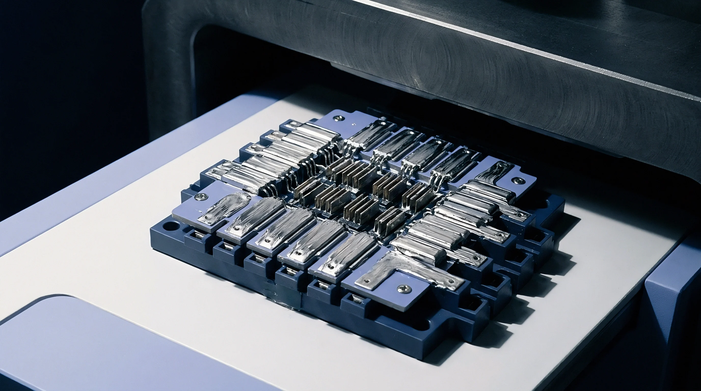
Comb
In silicon accelerometers, suspended micromachined proof masses use anchored interdigital fingers to build variable capacitors. When acceleration deflects the mass along its sensitive axis, the air gaps between the moving fingers and fixed frame electrodes change. This physical shift alters capacitance across opposing electrode pairs following standard parallel-plate electrostatics.
Most capacitive micro-electromechanical systems use differential topology to linearize transduction and cancel common-mode voltage noise.
Proof Mass Dynamics and Differential Geometry
External inertial forces translate directly into mechanical displacement across micron-scale silicon beams. Held by engineered flexures, the proof mass responds as a standard second-order system whose equation of motion balances inertial force against acceleration, structural damping, and spring stiffness.
Well below mechanical resonance, mass deflection stays linearly proportional to applied acceleration. Silicon springs exhibit linear behavior under low stress, giving predictable movement. Stiffer springs push up the natural frequency and widen bandwidth, but lower mechanical sensitivity.
Sizing the proof mass requires balancing volume against die real estate and etching limits.
Interdigital comb arrays boost total capacitance without needing a massive surface footprint. Tens or hundreds of parallel finger pairs connect electrically into two sensing capacitors with alternating gaps. As the mass shifts toward one set of fixed fingers, that gap narrows while the opposing gap widens by the exact same amount.
Capacitance per unit length is set by dielectric permittivity, overlap depth, and gap spacing. Standard single-crystal silicon processes yield high aspect ratios, with finger heights ten to twenty times greater than gap widths. This maximizes surface area and places baseline rest capacitance in the range of one to ten picofarads.
Gap-Closing versus Transverse Overlap Transduction
Varying gap distance yields higher sensitivity per unit area than shifting overlap area. Gap-closing layouts change the distance between parallel fingers while holding overlap area constant. Transverse overlap designs keep the gap width fixed and alter the lateral overlap length.
A single gap-closing finger pair has an inverse-distance capacitance curve, making its raw displacement response nonlinear. Subtracting the opposing capacitance pair linearizes the response to a first-order approximation, though cubic terms still emerge during large deflections.
Transverse overlap sensing yields a linear response across its range because capacitance scales directly with overlap length. However, unit-area sensitivity is lower because capacitance changes relative to nominal finger length rather than a micron-scale gap. High-precision accelerometers still lean toward gap-closing geometry for its superior signal-to-noise ratio, relying on differential processing or force-feedback loops to manage spatial nonlinearity.
Capacitive measurement subjects the suspended mass to continuous electrostatic forces. Applying a sensing voltage across narrow gaps generates an attractive force between moving and fixed fingers that scales inversely with the square of gap distance, introducing a negative electrostatic spring stiffness.
If measurement voltage rises too high, negative electrostatic stiffness overcomes the mechanical spring constant. At this pull-in threshold, moving fingers snap against stationary electrodes. Operating voltages must stay safely below pull-in limits to maintain mechanical stability and prevent physical contact.
Consider a 1.5 microgram proof mass suspended by flexures with an effective spring stiffness of 12 Newtons per meter. An acceleration of 10 g (98.1 meters per second squared) produces a mass displacement found by dividing inertial force by spring stiffness:
x = fracm · ak = frac1.5 × 10-9 kg × 98.1 m/s212 N/m = 12.26 πcometers
For an interdigital structure with 120 finger pairs, an overlap height of 30 microns, an overlap length of 100 microns, and a rest gap of 1.2 microns in air, nominal zero-g capacitance for one differential set is:
C0 = N · fracε0 · Ad0 = 120 · frac8.854 × 10-12 F/m × (30 μm × 100 μm)1.2 μm = 2.656 πcofarads
Under a 10 g displacement of 12.26 picometers, the differential capacitance change equals twice the nominal capacitance multiplied by the displacement ratio:
Δ C ≈ 2 · C0 · fracxd0 = 2 · 2.656 pF · frac12.26 × 10-12 m1.2 × 10-6 m = 54.3 femtofarads
This yields 5.43 femtofarads of differential capacitance shift per g of acceleration. Capturing these sub-femtofarad changes requires readout circuitry integrated alongside or directly on the sensor die.
Thicker proof mass structures increase mechanical sensitivity without expanding lateral silicon area.
Stiff flexures limit off-axis motion, suppressing mechanical cross-sensitivity. Off-axis forces can cause parasitic tilt or sliding that alters capacitance unpredictably. Folded-beam spring layouts decouple main axial movement from cross-axis tilt, holding cross-sensitivity below one percent of full scale.

Damping
Gas trapped inside sub-three-micron cavities resists proof mass motion through viscous drag. The gas around the moving comb fingers dictates dynamic response, settling time, and the mechanical noise floor. Managing this energy dissipation means setting internal cavity pressure precisely during wafer packaging.
Squeeze-Film Mechanics and Rarefied Gas Effects
As gap dimensions approach the mean free path of air, fluid flow behavior changes. Squeeze-film damping dominates gap-closing designs, pushing gas out and pulling it back during movement. These viscous resistance forces scale with the inverse cube of gap distance, rising sharply in narrow channels.
At higher vibration frequencies, gas compressibility adds a spring-like force component. Because fluid cannot escape the gap instantaneously, gas compresses between surfaces. Response shifts from low-frequency viscous damping to high-frequency elasticity, defined by the Cutoff Frequency parameter in Reynolds equation solutions.
Rarefied gas dynamics take over when the molecular mean free path approaches the gap width. The Knudsen number measures this rarefaction as the ratio of mean free path to gap thickness. In atmospheric air, the mean free path is about 68 nanometers, giving a Knudsen number around 0.057 across a 1.2-micron gap.
Above a Knudsen number of 0.01, standard continuum fluid models break down. Gas molecules strike microstructure walls more often than they hit each other, causing effective viscosity to fall below bulk values. Calculating drag accurately then requires slip-flow boundary corrections or Boltzmann kinetic transport models.
| Cavity Pressure (mbar) | Knudsen Number Range | Flow Regime | Mechanical Quality Factor (Q) | Noise Density (micro-g/sqrt-Hz) |
|---|---|---|---|---|
| 1013.25 (Atmospheric) | 0.01 to 0.10 | Slip Flow | 0.2 to 1.5 | 80.0 to 250.0 |
| 100.00 (Reduced) | 0.10 to 1.00 | Transition Flow | 2.0 to 12.0 | 15.0 to 60.0 |
| 1.00 (Vacuum Cavity) | 1.00 to 10.00 | Free Molecular | 50.0 to 500.0 | 1.0 to 8.0 |
| 0.01 (High Vacuum) | > 10.00 | Free Molecular | 2000.0 to 15000.0 | 0.1 to 0.8 |

Brownian Motion and Equivalent Noise Acceleration
Thermal agitation of gas particles creates random forces against the suspended structure. Continuous molecular impacts form a broadband mechanical noise floor, with thermal energy transferring directly into the sensor’s mechanical oscillation mode.
Under fluctuation-dissipation theory, mechanical damping inherently introduces noise. The energy loss mechanisms that dampen vibration also inject thermal noise. Equivalent noise acceleration spectral density depends on temperature, the damping coefficient, and proof mass:
an = sqrtfrac4 · kB · T · bm2 quad left
Lowering mechanical noise requires reducing the damping coefficient b or adding proof mass m. Extra mass drops physical noise but inflates die size and cost. Reducing cavity pressure lowers gas density, which cuts damping and drops mechanical noise density substantially.
However, low-pressure cavities leave sensors under-damped, creating sharp resonance peaks. Environmental vibration near the natural frequency can drive large deflections, saturating readout circuits or causing finger collisions. Designers balance noise targets against shock amplification, typically settling on a damping ratio near 0.707 for open-loop systems.
Baseline zero-g drift over device operating lifetimes often stems from pressure variance inside the micro-cavities.

Readout
Converting sub-femtofarad capacitance changes into clean digital data requires careful front-end amplification. Small capacitive cells present high source impedance, leaving traces vulnerable to board capacitance, electromagnetic interference, and leakage currents. Preserving resolution depends on co-designing the mechanical sensor with low-noise analog front ends.

Can Continuous-Time Readout Match Switched-Capacitor Noise Floors?
Continuous-time amplifiers consume less power at high frequencies but are prone to low-frequency flicker noise. These architectures apply high-frequency AC sine waves across differential plates to modulate capacitance shifts up to carrier frequencies, dodging 1/f noise before synchronous demodulators restore the baseband acceleration signal.
Switched-capacitor designs dominate automotive and industrial signal chains. Switches periodically transfer charge onto an integrating amplifier feedback loop. Anti-phase square waves drive the sensor plates, pushing differential charge into the summing node to turn capacitance changes into proportional voltages.
Correlated double sampling removes DC offsets and flicker noise by sampling amplifier noise during a reset phase and subtracting it from the signal phase. This leaves pure capacitive charge transfer, yielding conversion gain set by stable capacitor ratios rather than absolute resistor values.

Closed-Loop Force Rebalance Architecture
Closed-loop architectures use electrostatic drive pulses to hold the proof mass steady against inertial forces. Preventing physical deflection eliminates mechanical nonlinearity and extends measurement range far past open-loop limits.
Electromechanical sigma-delta loops treat the proof mass itself as a loop filter. The interface electronics digitize acceleration continuously, feeding bitstream pulse sequences back to drive electrodes that pull the mass back to null on every clock cycle.
Because pulse density tracks acceleration directly, the system outputs high-resolution digital data without a separate analog-to-digital converter. Dynamic range expands because flexures never reach non-linear deflection limits.
- Mechanical deflection initiation transfers force imbalances into physical displacement across interdigital comb elements.
- Differential charge injection drives unbalanced charge into amplifier summing nodes during active clock phases.
- Correlated sampling demodulation cancels transistor flicker noise while extracting phase-proportional baseband voltages.
- Sigma-delta loop quantizers evaluate integrated voltages to generate single-bit or multi-bit pulse-density output codes.
- Electrostatic feedback pulses apply proportional force to rebalance plates, pulling the proof mass back to center null.
The signal chain maps across physical and electronic domains through several distinct stages.
| Domain Stage | Physical Variable | Typical Dynamic Range | Primary Noise Source |
|---|---|---|---|
| Mechanical Mass | Acceleration to Deflection (10 ±/g) | 120 dB | Brownian Gas Collision Noise |
| Capacitive Comb | Deflection to Capacitance (5 fF/g) | 110 dB | Parasitic Fringing Capacitance |
| Charge Amplifier | Capacitance to Voltage (100 mV/fF) | 100 dB | Amplifier Input Thermal/Flicker Noise |
| Sigma-Delta Converter | Voltage to Bitstream Pulse Density | 96 dB to 120 dB | Quantization Noise / Clock Jitter |
A 24-bit electromechanical sigma-delta loop operating at 100 kilohertz sampling rates yields sub-micro-g resolution across 100 Hertz signal bandwidths.
High clock frequencies in switched-capacitor readouts risk injecting clock feedthrough currents into charge summing nodes, which can degrade noise performance if unmanaged.

Stress
Temperature shifts expand substrate materials at different rates. Molded plastic, die-attach adhesives, silicon substrates, and ceramic carriers each have distinct thermal expansion coefficients. Thermal changes induce stress gradients that propagate directly into the suspended flexures.

Packaging Mismatch and Substrate Deformation
Plastic mold encapsulation compresses the silicon die during cooling. As epoxy molding compound shrinks unevenly, it warps the underlying substrate. This bending distorts fixed comb fingers, shifting rest gaps even without applied acceleration.
Package stress distorts internal geometry over temperature, causing zero-g offset drift. Expressed in millig per Kelvin, the Temperature Coefficient of Offset tracks this shift. Thermal stress also alters spring stiffness, changing sensor sensitivity across operating temperatures.
Viscoelastic creep in die-attach adhesives causes long-term instability. As polymer adhesives slowly relax over time, they release stored mechanical strain. This relaxation manifests as baseline drift that single-point factory calibration at room temperature cannot eliminate.
- Polymer die-attach selection uses low-modulus silicone or soft epoxy formulations to absorb strain before it reaches the silicon die.
- Symmetrical substrate layout places proof masses along centerlines to cancel isotropic planar expansion forces.
- Stress-isolation anchor design attaches flexure suspensions to a single central pedestal, decoupling mechanics from substrate warpage.
- Hermetic ceramic carrier mounting replaces plastic encapsulation with cavity leadless chip carriers for high-stability uses.
Dielectric Charge Trapping Mechanisms
Under high electric fields, passivation oxides and insulating dielectric stoppers accumulate static charge over time. This trapped charge creates parasitic electrostatic fields that pull continuously on nearby proof fingers, driving persistent offset shifts.
Charge accumulation accelerates at higher temperatures and bias voltages, causing zero-g offsets to drift over hours of operation. Periodically reversing drive voltage polarity neutralizes this dielectric polarization, curbing long-term baseline drift.
| Package Type | Thermal Coefficient of Offset (mg/K) | Long-Term Drift (mg/1000h) | Moisture Sensitivity Level (MSL) | Relative Unit Cost Ratio |
|---|---|---|---|---|
| Molded Plastic LGA | ±0.5 to ±2.0 | 15.0 to 50.0 | MSL 3 | 1.0x |
| Cavity Plastic LGA | ±0.2 to ±0.8 | 5.0 to 15.0 | MSL 3 | 1.4x |
| Ceramic LCC (Hermetic) | ±0.05 to ±0.2 | 1.0 to 3.0 | MSL 1 | 3.8x |
| Wafer-Level CSP (WLCSP) | ±0.3 to ±1.2 | 8.0 to 25.0 | MSL 1 | 0.8x |
Standard industrial contracts stipulate that zero-g drift exceeding maximum datasheet bounds during assembly soldering triggers lot rejection at supplier cost.
Ignoring thermomechanical stress during board mounting leads to high calibration failure rates on assembly lines and zero-g drift in the field.

Qualification
Automotive and industrial standards require strict stress testing on production sensor lots. High-reliability applications demand proven survivability under environmental extremes before component adoption, exposing structural, chemical, and electrical vulnerabilities.

Automotive Reliability Protocols and Shock Limits
Vehicle stability platforms demand continuous operation despite thermal stress and vibration. AEC-Q100 and AEC-Q103 outline test sequences for automotive ICs and MEMS sensors, with AEC-Q103-002 specifying combined thermal cycling and mechanical shock requirements for micromachined accelerometers.
High Temperature Operating Life testing runs sensors at maximum rated ambient temperature for 1000 hours. Operating at 125 degrees Celsius or 150 degrees Celsius accelerates charge migration, electromigration, and package creep. Post-test evaluations flag any unacceptable offset shift or sensitivity drop.
Drop shock testing evaluates structural limits under extreme peak acceleration. Per ISO 16063-22, devices face half-sine pulses from 2000 g to 10000 g lasting less than a millisecond. Such sharp shocks can fracture silicon flexures, dislodge fingers, or cause stiction.
Stiction occurs when moving fingers contact stationary walls or substrates. Surface forces like van der Waals attraction or capillary action overpower mechanical restoration, trapping the mass. Anti-stiction coatings and mechanical travel stops limit contact area to prevent permanent lockup.

Electrostatic Self-Test Verification
Applying an internal DC bias across dedicated drive electrodes deflects the proof mass without physical motion. Integrated self-test routines use this to verify mechanical flexure mobility and signal chain continuity at startup.
Activating self-test applies an electrostatic force matching a calibrated g-level input. Interface logic confirms the output voltage shift falls within expected bounds; an unresponsive output indicates stiction, beam fracture, or amplifier failure.
- Pre-test baseline measurement registers zero-g offset voltage and stable temperature readings in environmental chambers.
- Thermal chamber ramp subjects units to 500 temperature cycles from minus 40 degrees Celsius to 125 degrees Celsius at controlled rates.
- Mechanical vibration exposure applies random vibration across three orthogonal axes for 24 hours per axis under active power bias.
- Post-stress functional evaluation tracks shifts in sensitivity, offset, self-test response, and supply current.
- Acceptance criteria audit verifies all parameters stay within end-of-life datasheet limits without structural failure.
Integrated electrostatic self-test routines verify mechanical structural integrity without requiring physical rotation test benches.
Standard AEC-Q103-002 Grade 1 mandates that zero-g offset drift stay within strict limits across the minus 40 to 125 degrees Celsius operating range.
Allocation
Fab capacity and specialized packaging dictate component availability for silicon sensors. Capacitive MEMS relies on dedicated surface or bulk micromachining nodes. Because foundries use custom process steps, porting designs between fabs during market shortages is difficult.

Wafer-Level Capping and Foundry Dependency
Fragile silicon suspensions are hermetically sealed before dicing to shield them from contamination. Wafer-level capping bonds a cover wafer over the MEMS device wafer in cleanrooms, forming hermetic cavities over the proof mass.
Aluminum-Germanium eutectic bonding and glass frit bonding are the primary capping methods. Glass frit bonding requires high thermal budgets near 430 degrees Celsius, introducing stress into the silicon array. Eutectic bonding operates at lower temperatures with narrow seal rings, keeping package stress and die footprint smaller.
Through-Silicon Vias (TSVs) connect through the wafer cap directly to external ball grid arrays. Eliminating long wire bonds reduces parasitic capacitance and package height. However, TSV processing requires advanced deep reactive ion etching and precise wafer alignment, limiting manufacturing options to specialized MEMS foundries.

Second-Source Equivalency and Pin Compatibility
Alternate vendors rarely match substrate layouts, register maps, or pinouts exactly. Because sensor designs depend heavily on specific mechanical geometries and custom ASIC signal chains, changing part numbers usually requires board redesigns and firmware updates.
Package footprint compatibility does not guarantee drop-in signal equivalency. Pin-compatible alternatives often differ in noise spectral density, bandwidth settings, settling time, or I2C/SPI register maps, requiring thorough cross-qualification testing across operating conditions.
Sole-sourcing a proprietary accelerometer leaves high-volume products vulnerable to fab downtime. Effective multi-sourcing relies on components built on standard multi-client MEMS foundry platforms paired with pin-compatible interface electronics.
Securing multi-foundry allocation requires validating secondary fabs early in development. Minor geometry variations between foundries alter comb finger etch profiles, shifting spring constants and baseline capacitance. Qualifying a second source means recalibrating ASIC charge-amplifier gains and filter coefficients to match full-scale sensitivity and thermal offset performance across both supply chains.