Silicon Pressure Sensor Package Stress Isolation Methods
Mechanical stress isolation via matched CTE submounts, compliant gels, and silicon micro-machined trenches eliminates parasitic packaging strain to preserve long-term sensor calibration stability.


Header
Piezoresistive and capacitive silicon pressure sensor elements convert microscopic lattice strain into electrical signals with high sensitivity. That same physical response makes the sensor die sensitive to mechanical forces from the surrounding package stack. When a silicon die with a thermal expansion coefficient near 2.6 ppm per degree Celsius is bonded to a substrate with a different expansion rate, temperature shifts create planar strain across the active diaphragm.
This thermo-mechanical strain causes zero-point offset shift, full-scale span drift, non-linearity, and thermal hysteresis that cannot be distinguished from actual fluid pressure changes.
Package headers act as the structural anchor and media interface for the sensor assembly. The choice of header alloys, ceramic compositions, and glass isolation feedthroughs sets the strain baseline for the instrument. Headers machined from austenitic stainless steel have thermal expansion coefficients around 16 ppm per degree Celsius, which creates severe mismatch stress directly at the die attachment boundary.
Advanced isolation designs use intermediate materials to step down these stress gradients across the interface layers.
Borosilicate glass pedestals, formulated to match the thermal expansion profile of silicon, serve as primary stress-decoupling anchors. Anodic bonding directly joins the back surface of the silicon die to the glass pedestal at elevated temperatures, typically near 400 degrees Celsius, creating a hermetic, monolithic joint with minimal residual strain. The pedestal’s thickness and aspect ratio determine how effectively it attenuates substrate-induced bending moments before those forces reach the piezoresistive bridge.
Header body materials dictate how mounting torque and pipe strain transfer to the internal sensor cavity. Machined Kovar alloys match the thermal expansion of borosilicate glass across standard industrial operating ranges, preserving the interface during severe thermal shock. Low-temperature co-fired ceramic headers offer an alternative, allowing embedded electrical interconnects and tailored thermal expansion profiling within a rigid, low-creep body.
| Material Stack Layer | Coefficient of Thermal Expansion (ppm/K) | Young’s Modulus (GPa) | Poisson Ratio | Interfacial Stress Impact |
|---|---|---|---|---|
| Single-Crystal Silicon Die | 2.6 | 130 to 169 | 0.28 | Active transducer baseline |
| Borosilicate Glass Pedestal | 3.25 | 64 | 0.20 | Primary stress attenuation layer |
| Kovar Alloy (Fe-Ni-Co) Header | 5.1 to 5.5 | 138 | 0.31 | Low-mismatch structural housing |
| Low-Temperature Co-Fired Ceramic | 5.8 to 7.0 | 110 to 120 | 0.24 | Planar routing and intermediate substrate |
| 316L Stainless Steel Header | 16.0 to 16.5 | 193 | 0.30 | High mismatch requiring compliant isolation |
Directly soldering silicon or glass-mounted dies to metal headers creates localized stress points as the solder creeps and intermetallic grains grow over time. Lead-tin and gold-tin eutectic alloys form tight hermetic seals, but their higher elastic moduli transmit structural distortion into the silicon matrix. Softer solders undergo continuous microstructural relaxation, turning mechanical stress into long-term zero drift during field operation.
Glass-to-metal seals around header feedthrough pins introduce secondary stress pathways. Differential cooling during header fabrication leaves compressive stress trapped in the glass matrix around electrical leads. When terminal pins experience mechanical loads during wire bonding or harness connection, these residual stresses shift within the header body, shifting the die mounting plane by sub-micron amounts.
These tiny displacements produce measurable zero shifts in low-pressure piezoresistive diaphragms, where full-scale mechanical deflections are only a few hundred nanometers.
Header isolation relies on geometric isolation channels as well as CTE matching. Circumferential isolation slots machined into metal headers physically separate the central die mounting island from the outer threaded body. Thread engagement torque during transmitter installation deforms the outer housing, but the compliance of the isolation slot absorbs elastic strain energy before it reaches the submount plane.
Zero-point drift originating from unmitigated header thermal mismatch often exceeds two percent of full-scale output across a one-hundred-degree operating window.
Isolating mounting stress requires tight control of surface flatness and parallelism across every mating interface in the package stack. Lapping and polishing header surfaces to sub-micron tolerances eliminates localized stress risers from point contacts. If a sensor pedestal rests on an uneven header surface, clamping forces produce asymmetric bending stresses that rotate the principal stress axes within the silicon crystal plane.
This rotation alters piezoresistive coefficients, corrupting the temperature compensation matrix set during factory calibration.
Failure to isolate the package header from external assembly forces degrades sensor performance far beyond initial calibration limits. Field instruments subject to heavy pipe strain or high installation torque show unpredictable zero-point wander that defies electronic zero correction. Misaligned thermal expansion coefficients across the submount stack cause irreversible plastic deformation in soft die-attach layers, permanently compromising long-term measurement stability.

Gel
Potting materials and encapsulation media protect active silicon sensor faces from corrosive process fluids while passing external hydraulic pressure to the measuring diaphragm. Silicone gels, fluorosilicone formulations, and gel-filled cavities create a soft mechanical interface that insulates the micro-machined diaphragm from direct physical contact with aggressive media. The physical mechanics of these dielectric gels govern both media compatibility and parasitic stress transmission to the active piezoresistive bridge.
Extremely low shear modulus values allow silicone encapsulation gels to deform freely under applied pressure, transferring fluid stress to the silicon surface without adding localized structural constraint. Standard encapsulation gels have Young’s moduli below one hundred kilopascals, compared to the gigapascal-scale stiffness of the silicon substrate. This stark difference in stiffness ensures that fluid pressure translates accurately into uniform normal stress across the diaphragm, while lateral thermal expansion forces within the gel dissipate through volumetric displacement.
Bulk thermal expansion of dielectric gels creates a secondary stress vector at temperature extremes. Silicone gels have volumetric thermal expansion coefficients near 900 ppm per degree Celsius, roughly three hundred times higher than single-crystal silicon. In sealed sensor cavities, constrained expansion of the gel builds parasitic internal hydrostatic pressure that loads the sensor diaphragm independently of applied media pressure.
This thermally induced hydrostatic pressure produces a severe non-linear temperature coefficient of zero.
- Volumetric expansion confinement creates parasitic hydrostatic pressure in sealed sensor cavities at elevated temperatures, driving zero-point offset errors that vary non-linearly with temperature.
- Gel swelling via solvent absorption alters the cross-link density and volume of the encapsulant, generating swelling forces that apply asymmetric shear strain across wire bonds and piezoresistor traces.
- Low-temperature glass transition solidification turns soft silicone compounds into rigid solids below minus forty degrees Celsius, sharply elevating shear modulus and transferring heavy packaging stress directly to the silicon diaphragm.
- Outgassing bubble formation during vacuum operation or high-temperature processing traps gas bubbles against the diaphragm surface, altering local compliance and causing step-changes in sensitivity calibration.
Soft gel encapsulants alter the dynamic response of pressure sensors through viscous damping. At higher temperatures, gel viscosity drops, allowing high-frequency pressure fluctuations to pass through to the diaphragm unattenuated. At sub-zero temperatures, gel viscosity rises exponentially, introducing phase lag and amplitude attenuation into dynamic measurements.
Design engineers balance acoustic impedance matching against dynamic response bandwidth when setting gel fill volumes and geometries.
Fluorosilicone gels offer better chemical resistance against hydrocarbon solvents, fuels, and acidic industrial condensate than dimethyl silicone formulations. However, fluorosilicone materials have higher density and slightly higher stiffness, increasing low-temperature thermal stress transfer. Fluorosilicone polymer chains also exhibit higher dielectric constants, raising parasitic capacitive coupling risks when applied directly over unpassivated high-impedance circuitry or capacitive sensing electrodes.
Interfacial adhesion between the encapsulation gel and sensor die passivation prevents moisture ingress along the die surface. Loss of adhesion creates micro-voids where water vapor collects, forming localized condensation sites during ambient temperature cycles. Free water beneath the gel layer causes localized electrochemical corrosion on aluminum wire bond pads and alters local stress distribution across the active sensing elements.
Dispensing procedures for soft gels set the initial strain state within the packaged cavity. Automated needle dispensing requires precise volume control to keep a consistent fill height relative to the diaphragm surface. Overfilling the gel cavity increases structural confinement stress against the package lid, whereas underfilling leaves wire bond loops exposed to fluid shear forces during high-flow pressure transients.
Vacuum degassing removes micro-bubbles from the gel matrix prior to thermal curing, preventing localized pressure anomalies during operation.
Dual-gel encapsulation architectures mitigate chemical attack while preserving low-stress conditions across the silicon diaphragm. An ultra-soft primary gel layer coats the silicon surface to provide stress-free passivation, while a denser, fluorinated secondary gel fills the upper cavity as a barrier against aggressive chemicals. The compliance of the primary gel decouples the die from stress generated by the stiffer outer barrier layer.
Compliance variation across gel manufacturing batches presents persistent calibration challenges in precision pressure instruments. Standard penetration tests measure gel consistency, but small variations in cross-link density cause measurable shifts in low-temperature stiffness. Sensor manufacturers find that batch-to-batch variations in gel cure kinetics translate directly into zero-point thermal coefficient shifts across production lots.
Gel formulation changes frequently force re-qualification of packaging stress isolation baselines across industrial sensor lines. When chemical suppliers modify catalyst systems or resin purity, the long-term stress relaxation behavior of the cured gel changes silently. Material datasheets report bulk hardness and dielectric strength, but routinely omit long-term creep modulus and thermal stress relaxation dynamics under continuous mechanical strain.
Trench
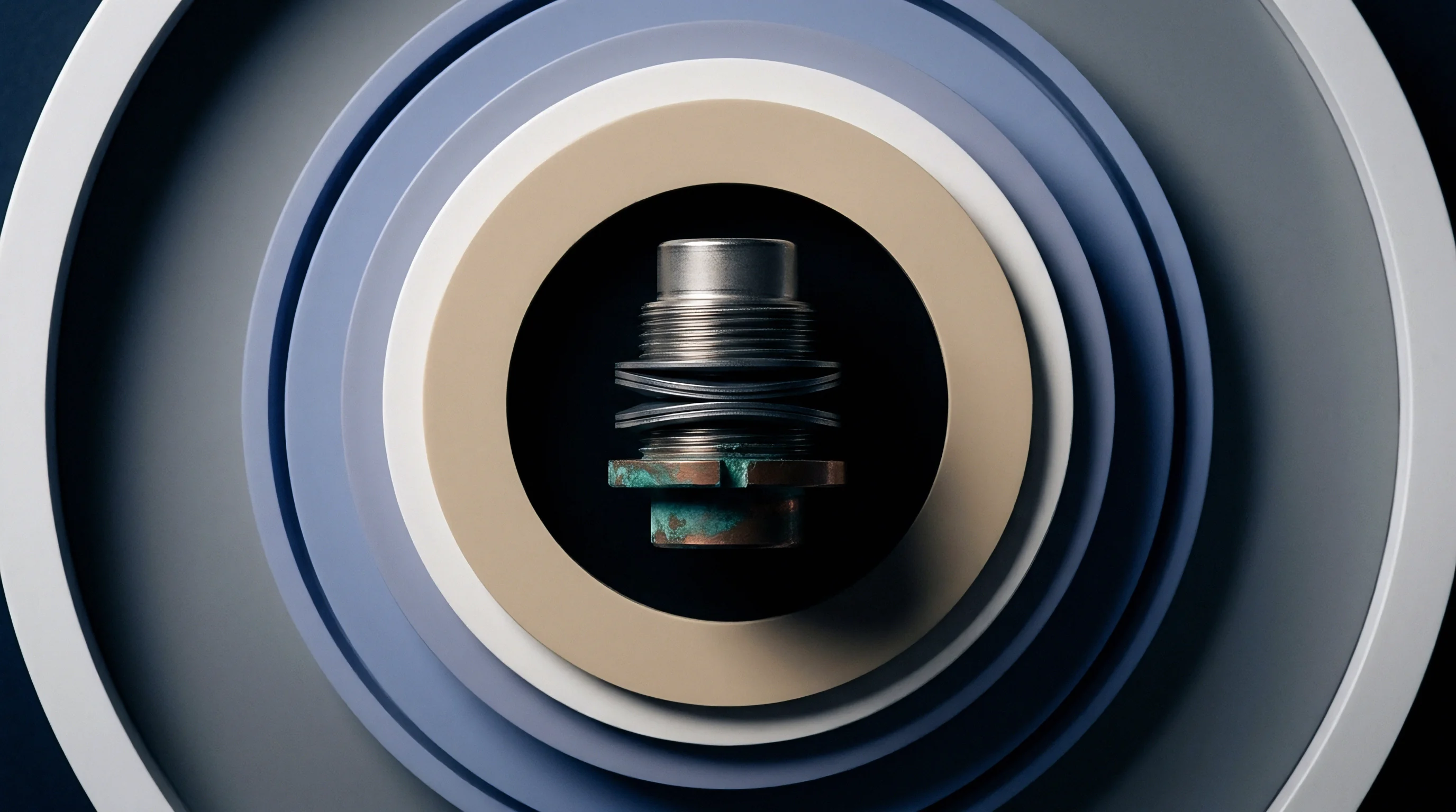
Backside micromachining techniques integrate stress-isolation geometries directly into the silicon substrate, physically decoupling the active piezoresistive sensing area from package-induced stresses. Deep reactive ion etching creates isolation trenches, annular slots, and compliant beam structures within the silicon die layout itself. Moving mechanical compliance from external packaging adhesives into the single-crystal silicon matrix eliminates the long-term creep and viscoelastic relaxation inherent to polymeric isolation materials.
Deep silicon trenches around the central pressure diaphragm route package mounting strain away from the active transducer area. Mechanical strain propagating inward from the die-attach perimeter encounters the high-aspect-ratio trench, which acts as a mechanical open circuit. The structural compliance of the thin silicon walls within the trench absorbs planar strain energy, attenuating packaging stress before it reaches the piezoresistors on the central diaphragm.
Etch geometry parameters determine how effectively substrate isolation features attenuate stress. Deep trenches extending through eighty percent of the substrate thickness achieve dramatic reductions in transmitted stress while preserving structural strength against burst pressure limits. Aspect ratios exceeding twenty-to-one allow narrow trench footprints that maximize active diaphragm area while providing effective isolation against out-of-plane bending moments.
Gimbaled die architectures represent an advanced evolution of trench-based stress isolation. Outer silicon rings attach directly to the package substrate using conventional adhesives, while inner sensing diaphragms suspend from thin, micro-machined silicon flexure beams. Mechanical distortion of the outer ring deforms the flexure beams, leaving the central sensing island free from parasitic bending strain.
This configuration isolates the active transducer from thermal expansion mismatch, substrate warping, and die-attach voiding stresses simultaneously.
Incorporating deep isolation trenches into silicon sensor dies reduces thermo-mechanical package stress transmission by more than eighty-five percent across industrial operating temperature ranges.
Anisotropic wet etching using potassium hydroxide or tetramethylammonium hydroxide forms inclined sidewalls following the crystal planes of single-crystal silicon. While wet-etched isolation trenches carry lower manufacturing costs than deep reactive ion etching, their crystallographic angle constraints demand more die real estate. Sidewall angles of 54.7 degrees in standard silicon wafers broaden the trench footprint, increasing die size and lowering per-wafer net yield.
Stress concentration at the internal roots of micro-machined trenches poses fracture mechanics risks under high shock or overpressure events. Sharp internal corners created during dry etching concentrate mechanical stress, serving as nucleation sites for micro-cracks under severe cyclic loading. Isotropic surface smoothing etches or thermal oxidation passes round these internal corner radii, redistributing stress concentrations and raising fracture toughness without compromising structural strain isolation.
Bulk micromachining of backside stress-relief cavities requires precise front-to-back wafer alignment. Isolation trenches must align accurately relative to frontside piezoresistor networks to maintain symmetric stress distribution across the Wheatstone bridge. Misalignment between frontside lithography and backside trench patterns creates structural asymmetry, causing planar packaging stresses to turn into parasitic shear strains that degrade bridge balance and cross-axis sensitivity.
Dual-diaphragm structures use an outer thick diaphragm to absorb mounting stresses while an inner thin diaphragm carries out the primary pressure measurement. The outer diaphragm frame acts as an integrated stiffening ring anchoring the die to the submount, preventing edge boundary deformations from propagating into the central thin diaphragm region. This structural hierarchy delivers superior zero-point stability under high static line-pressure conditions in differential pressure applications.
Surface micromachined strain isolation channels rely on thin-film surface layers rather than full substrate etching. Polysilicon or monocrystalline silicon micro-bridges suspend above sacrificial oxide cavities, isolating sensitive resonant or capacitive structures from bulk substrate deformation. These surface features decouple localized high-frequency sensing elements from low-frequency structural vibration and package thermal strain, though their application remains restricted to low-pressure atmospheric and environmental monitoring.
Etch profile variations across silicon wafers introduce subtle changes in isolation beam compliance. Micro-loading effects during deep reactive ion etching cause trench depths to vary between dense central regions and sparse wafer peripheries. These depth variations shift the mechanical stiffness of stress-isolation flexures, altering sensitivity and stress isolation performance across a production run.
Integrating complex trench geometries into silicon pressure sensor dies increases front-end wafer processing costs substantially. Additional lithography masks, backside deep etching steps, and specialized wafer handling raise raw die costs by forty to sixty percent. Instrument designers must weigh whether this front-end silicon expense offsets the back-end packaging costs of multi-layer header assemblies and high-precision adhesive dispensing.
Questions remain regarding high-frequency resonant modes introduced by highly compliant micro-machined isolation flexures in severe vibration environments. When external shock frequencies match the natural frequency of the suspended central die island, dynamic amplification can cause structural contact between the die and surrounding package walls. Engineers continue to evaluate whether mechanical stops or viscoelastic dampening media within the trench cavity provide enough dampening without re-introducing low-temperature thermal stress bridges.


Compliance
Polymeric die-attach adhesives and elastomeric mounting elements provide compliant mechanical interfaces that absorb differential thermal expansion between silicon sensor elements and package substrates. High-modulus epoxy adhesives transmit package strain directly into the silicon die, causing severe thermal zero shifts. Compliant silicone, fluorosilicone, and modified polyurethane die-attach materials isolate the active sensor by deforming elastodynamically under strain, preventing stress transfer across the bond line.
Glass transition temperature sets the operational window where die-attach compliance remains effective. Above their glass transition temperature, amorphous polymers exhibit low elastic moduli and high compliance, accommodating thermal expansion mismatches with minimal stress transfer. Below the glass transition region, polymer chain mobility freezes, causing elastic modulus to jump by two to three orders of magnitude.
A compliant die-attach adhesive that effectively isolates stress at room temperature becomes a stiff, stress-transmitting solid at sub-zero industrial temperatures.
Thickness control across the adhesive bond line determines mechanical isolation performance and tilt angle alignment. Extremely thin die-attach layers, below ten microns, lack sufficient shear volume to absorb differential CTE movement, leading to high interfacial shear stress and potential adhesive failure. Excessively thick bond lines, exceeding one hundred microns, introduce die tilt and planar instability, causing the sensor die to shift position under external shock and vibration.
Viscoelastic creep in compliant adhesives introduces long-term zero-point stability risks. When a compliant adhesive experiences continuous stress from temperature mismatch or package distortion, the polymer chains slowly realign over time. This stress relaxation process converts elastic strain energy into permanent plastic deformation, causing the zero-point offset of the sensor to drift continuously over months or years of field service.

When Does Geometric Decoupling Fail under High Pressure?
High static line pressure compresses compliant die-attach materials, altering their effective mechanical compliance and stress isolation properties. Under elevated hydrostatic pressure, free volume within the polymer matrix collapses, causing bulk stiffness to increase significantly. This pressure-induced stiffening degrades the adhesive’s capacity to absorb concurrent thermal expansion strains, re-coupling package stresses directly to the silicon transducer during high-pressure operating cycles.
- Dispense compliant silicone die-attach material onto the prepared submount surface using a controlled cross-pattern matrix to prevent gas trapping.
- Place the silicon pedestal assembly onto the wet adhesive matrix using automated pick-and-place equipment with regulated bond force to control squeeze-out.
- Verify bond line thickness and tilt alignment using optical inspection or low-power X-ray imaging before thermal processing.
- Execute a multi-stage thermal curing cycle with low temperature ramp rates to promote complete cross-linking while minimizing void formation from solvent evaporation.
- Inspect cured bond lines for edge fillets and perimeter voiding to ensure uniform mechanical stress distribution across the die base.
Voiding within the die-attach layer breaks interfacial stress symmetry across the base of the silicon die. Trapped air pockets or solvent outgassing bubbles form non-uniform compliance regions beneath the sensor mount. When the package expands thermally, areas above solid adhesive experience continuous shear strain, while areas above voids remain unconstrained.
This localized stress gradient warps the silicon substrate, inducing zero offset shifts and non-linearity that vary non-monotonically with temperature.
Silicone die-attach formulations feature elastic moduli between 0.5 and 5.0 megapascals, providing exceptional mechanical stress isolation across broad temperature spans. However, low surface energy and poor tensile strength limit their load-bearing capacity under high shock loading conditions. Modified epoxy resins engineered with soft rubbery phases attempt to bridge this performance gap, offering moderate compliance alongside high cohesive strength for severe aerospace applications.
Compliant die-attach materials must maintain their elastic modulus below ten megapascals across the entire operational temperature range to prevent thermal stress transfer.
Silicone outgassing poses contamination risks for sensitive optical, capacitive, or micro-relay contacts enclosed within the same hermetic package cavity. Volatilized siloxane species condense on cold surfaces, forming insulating dielectric films that degrade electrical contact resistance and alter optical window transmission. Vacuum baking and high-purity space-grade low-outgassing silicone formulations limit volatile condensable material content to acceptable levels.
Floating O-ring package designs achieve physical stress isolation by suspending the sensor assembly between elastomeric seals rather than bonding it directly to a rigid submount. Fluid pressure acts upon the front face of the floating sensor module, while internal O-rings provide dynamic pressure sealing alongside mechanical compliance. Pipe stress, assembly torque, and package thermal expansion dissipate within the elastomeric deformation of the O-rings, leaving the internal silicon sensor element completely free from structural strain.
Temperature-dependent modulus tracking reveals significant mechanical hysteresis in compliant polymer mounts subjected to cyclic thermal loading. As temperature rises and falls, polymer chain relaxation rates lag thermal inputs, producing distinct stress pathways during heating and cooling phases. This mechanical hysteresis translates directly into measurement hysteresis, where sensor output at a specific temperature depends upon whether the instrument arrived from a higher or lower temperature baseline.
Matching die-attach cure profiles to production batch parameters limits internal residual stress built during manufacturing. Rapid thermal curing creates non-uniform cross-link density and high thermal gradients across the adhesive layer, locking mechanical stress into the bond line upon cooling. Slow, ramped cure profiles allow polymer chains to relax completely during cross-linking, yielding a strain-free baseline mount prior to initial sensor calibration.
A safe rule of thumb for compliant packaging design dictates that the die-attach bond line thickness should match or exceed five percent of the total die edge length to ensure adequate shear strain absorption.

Verification
Establishing the efficacy of stress isolation methods requires specialized metrological verification protocols designed to isolate package-induced thermal and mechanical strain from true pressure responses. Standard multi-point pressure calibrations fail to separate parasitic packaging stress from intrinsic transducer non-linearity. Advanced testing protocols combine environmental thermal cycling, structural mounting torque challenges, spatial strain mapping, and long-term zero drift monitoring to validate packaging performance.
Thermal zero hysteresis testing serves as the primary diagnostic tool for identifying interfacial packaging stress and creep within die-attach materials. The verification protocol subjects packaged pressure sensors to repeated thermal profiles across their full operating range, stopping at designated temperature dwell points to measure unpressurized zero-point output. Divergence between heating and cooling zero profiles exposes mechanical hysteresis resulting from adhesive viscoelasticity, structural yield in solder joints, or friction across sliding package interfaces.
Installation torque sensitivity testing quantifies the isolation efficiency of external header and housing designs. Sensors are installed into rigid test fixtures using calibrated torque wrenches across a range extending from fifty percent below to fifty percent above specified installation values. Real-time monitoring of zero-point offset during torque application reveals whether external thread deformation and body strain propagate inward to the silicon sensing element.
| Uncertainty Contribution Source | Standard Uncertainty Value | Probability Distribution | Sensitivity Coefficient | Combined Uncertainty Impact (% FSS) |
|---|---|---|---|---|
| Reference Pressure Controller Stability | 0.003 % Span | Normal (k=2) | 1.0 | 0.0015 |
| Thermal Chamber Temperature Gradient | 0.15 °C | Rectangular | 0.010 % FSS/°C | 0.0009 |
| Digital Multimeter Readout Resolution | 0.2 µV | Normal (k=1) | 0.001 % FSS/µV | 0.0002 |
| Fixture Thread Strain Coupling | 0.025 % FSS | Rectangular | 1.0 | 0.0144 |
| Die-Attach Viscoelastic Creep Residual | 0.018 % FSS | Triangular | 1.0 | 0.0073 |
Digital image correlation and optical interferometry provide non-contact, spatial mapping of planar deformation across active sensor diaphragms during thermal and mechanical loading. By tracking surface speckle patterns through glass-windowed environmental chambers, optical tools quantify sub-micron structural displacements induced by packaging stress. These empirical strain maps validate finite element stress models, verifying whether isolation trenches and compliant submounts perform according to theoretical strain decoupling predictions.
Accelerated thermal aging protocols evaluate long-term zero drift mechanisms associated with adhesive curing, stress relaxation, and intermetallic compound growth. Sensors undergo continuous elevated temperature storage, typically at 125 or 150 degrees Celsius, for durations ranging from one thousand to five thousand hours. Intermittent zero-point calibrations record offset drift over time, allowing metrologists to extrapolate three-year stability figures and identify premature packaging degradation mechanisms before product release.
Environmental humidity testing isolates moisture-induced stress mechanisms within polymeric encapsulants and die-attach adhesives. Polyimide passivations and silicone gels absorb atmospheric moisture, resulting in volumetric swelling and dielectric constant alterations. Subjecting sensors to eighty-five degrees Celsius and eighty-five percent relative humidity for one thousand hours exposes swelling-induced zero shifts, enabling engineers to distinguish between mechanical packaging strain and chemical degradation of protective coatings.
High-g mechanical shock and random vibration testing evaluate structural robustness without sacrificing compliance. Compliant die-attach mounts and gimbaled trench structures must maintain structural integrity when exposed to MIL-STD-883 acceleration profiles exceeding one thousand g. Post-shock calibration passes verify whether mechanical stress isolation structures survived without plastic deformation, structural micro-cracking, or permanent alignment shifts.
- Thermal dwell stabilization time must exceed thirty minutes per temperature step during hysteresis characterization to ensure complete thermal equilibrium across internal package stack layers.
- Pressure reference line isolation prevents small ambient pressure changes from contaminating zero-point stress drift measurements during long-term environmental chamber evaluations.
- Excitation voltage ratiometric tracking eliminates power supply drift uncertainties from high-precision zero-point stability recordings across extended testing cycles.
- Atmospheric pressure compensation requires continuous barometric monitoring or absolute pressure reference tracking when testing vented gauge pressure sensors over extended time horizons.
Static line pressure sensitivity testing in differential pressure sensors isolates common-mode structural distortion from true differential pressure signals. High static pressures, reaching hundreds of bar, compress the sensor housing and submount assembly. Proper stress isolation ensures that this high background pressure does not induce asymmetric strain across the differential sensing diaphragm, which would manifest as line-pressure zero shift and span error.
Rigorous uncertainty budgeting ensures that measurement facility limits do not mask subtle stress isolation defects. Thermal chamber gradients, reference standard drift, and mounting fixture compliance contribute measurement uncertainties that must remain an order of magnitude smaller than the target sensor stability tolerance. A sensor accuracy claim of 0.05 percent full scale demands a test system uncertainty baseline below 0.005 percent across the complete thermal evaluation window.
Field verification data collected from deployed sensor fleets provides the ultimate test for package stress isolation architecture. Continuous monitoring of zero-point calibration adjustments in automated processing plants reveals whether packaging stress relaxation continues over years of thermal cycling. Comparing bench test predictions against field return data identifies unmodeled stress interaction pathways, driving continuous refinement of packaging design baselines.
Clause 6.3 of ISO/IEC 17025 dictates that environmental conditions, mounting arrangements, and calibration histories must be recorded during uncertainty evaluations, ensuring that packaging stress artifacts remain fully traceable across laboratory comparisons.

Outlay
Designing and implementing stress isolation architectures introduces trade-offs between unit bill of materials cost, manufacturing complexity, assembly yields, and long-term warranty exposure. Low-cost industrial pressure sensors utilize direct epoxy bonding onto metal headers, accepting severe thermal zero shifts to minimize initial manufacturing expense. High-precision process transmitters incorporate multi-layer isolation stacks, micro-machined silicon trenches, and high-purity gel encapsulation, driving package costs up by orders of magnitude to secure long-term measurement stability.
Silicon die area consumption represents a primary cost driver when incorporating internal stress-isolation features. Backside isolation trenches, gimbal rings, and compliant support beams increase total die surface area by thirty to one hundred percent compared to basic un-isolated diaphragm layouts. Because semiconductor wafer costs remain fixed per run, larger die footprints directly reduce the number of net good die per wafer, elevating raw transducer chip costs proportionally.
Submount material processing adds significant expense to high-performance sensor packages. Precision-ground borosilicate glass pedestals require diamond sawing, ultra-sonic drilling, and double-sided polishing to achieve micro-inch flatness specifications. Anodic bonding processes require specialized vacuum equipment, high voltage supplies, and elevated temperature controls, adding processing time and capital depreciation costs to every manufactured submount lot.
Automated assembly yield rates reflect the manufacturing complexity of compliant packaging architectures. Soft silicone die-attach materials present challenging dispensing tolerances, where small variations in fluid viscosity, needle tip height, or ambient humidity lead to bond line voiding, die tilt, or squeeze-out contamination onto active wire bond pads. Lower yield rates during back-end packaging steps carry heavy cost penalties, as defective units contain fully processed silicon dies and precision machined headers.
| Isolation Architecture Grade | Packaging Cost Multiplier | Thermal Zero Drift (% FSS / 100°C) | Assembly Yield Impact (%) | Target Application Market |
|---|---|---|---|---|
| Direct Epoxy on Steel Header | 1.0x (Baseline) | 1.5 to 3.0 | 98.5 | HVAC, Consumer Hydraulics |
| Glass Pedestal on Kovar Header | 2.8x | 0.25 to 0.50 | 95.0 | Industrial Process Control |
| Silicon Trench + Compliant Gel | 4.5x | 0.05 to 0.15 | 91.0 | Custody Transfer, Aerospace |
| Floating O-Ring / Gimbaled Architecture | 7.2x | 0.01 to 0.05 | 86.0 | Metrology, Secondary Standards |
Calibration overhead costs escalate rapidly when packaging stress isolation remains incomplete. Sensors exhibiting high thermal zero hysteresis require complex, multi-point thermal calibration cycles inside environmental chambers to generate individual polynomial compensation matrices. Extended thermal chamber dwell times consume factory floor capacity, energy, and capital, representing up to forty percent of total finished unit manufacturing outlay.
Superior physical stress isolation reduces thermal hysteresis to levels where simple two-point room-temperature trim processes achieve target specifications, drastically lowering factory calibration line expenditure.
Warranty exposure and field re-calibration service budgets shift the commercial evaluation toward investment in robust stress isolation. Sensors installed in remote, hazardous, or subsea locations incur field service replacement costs that dwarf initial instrument acquisition prices. A sensor that drifts out of specification due to packaging stress relaxation forces unscheduled plant downtime and expensive field re-calibration technician visits.
Investing in low-stress packaging architectures upfront protects manufacturers against costly warranty recalls and long-term brand reputation damage.
Secondary processing costs include specialized handling and extended burn-in protocols required for compliant packaging polymers. Soft die-attach materials demand high-temperature thermal stabilization bakes lasting twenty-four to forty-eight hours to complete cross-linking and accelerate early viscoelastic stress relaxation before final factory calibration. These burn-in steps increase work-in-progress inventory holding costs and extend production cycle times across manufacturing facilities.
Supplier selection strategies balance component piece-part costs against quality assurance capabilities. Header machining vendors must maintain tight statistical process control over alloy compositions, plating thicknesses, and thread tolerances to prevent non-conforming parts from introducing unexpected mounting stress anomalies into production lines. Sourcing practices prioritize vendors capable of delivering fully certified, lapped headers with full material batch traceability over low-bid suppliers whose dimensional variations compromise assembly yields.
The total cost of ownership model demonstrates that high-precision measurement applications justify premium packaging stress isolation expenditures. When measurement uncertainty directly impacts commercial billing, such as oil and gas custody transfer or chemical dosing accuracy, the economic returns of long-term zero stability easily outweigh initial sensor packaging costs. Precision packaging transforms micro-machined silicon elements into robust, traceable metrological instruments capable of maintaining tight tolerances across years of un-serviced industrial operation.