Electrical Translation
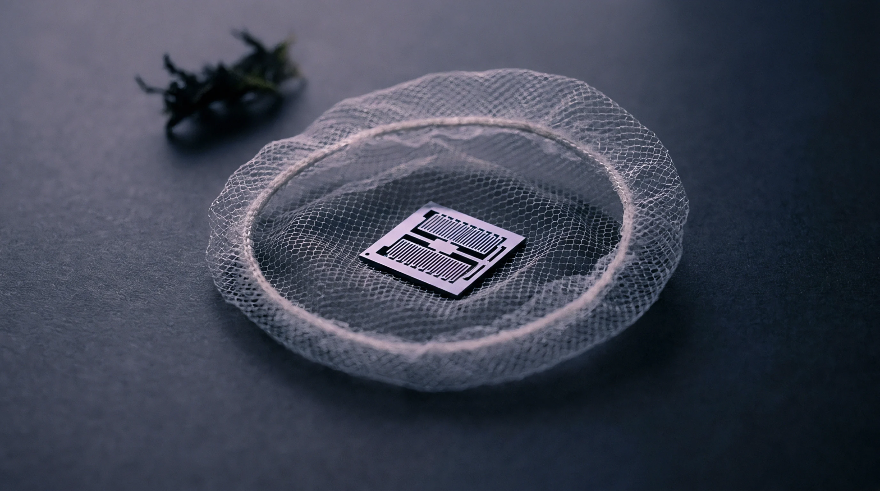
Crystal lattice deformation alters semiconductor resistivity through internal mechanical stress, forming the basis of piezoresistive strain measurement. External mechanical loads deflect the host material, shifting carrier mobility within doped silicon domains. The resulting resistance variance scales proportionally with applied mechanical displacement until material yield limits interrupt signal linearity.
Transducers convert this resistance shift into a proportional voltage change using balanced Wheatstone bridge circuits powered by regulated excitation sources. Calibration protocols verify output accuracy against reference dead weight standards under controlled thermal baselines. Metrologists establish zero balance points before testing begins to eliminate initial offset errors from the final calculation.
Environmental temperature fluctuations introduce thermal drift that requires active compensation resistors to maintain measurement integrity.
Crystal Deformation
Atomic bond stretching produces carrier scattering inside the semiconductor crystal lattice during mechanical loading. Semiconductor doping concentrations determine gauge factor magnitude and establish the usable operational ceiling for the sensing element. High gauge factors deliver substantial signal output relative to metallic foil alternatives, yet introduce greater thermal sensitivity across operating temperature ranges.
Carrier mobility drops as lattice temperatures rise, shifting output curves downward unless compensation networks correct the voltage signal. Piezoresistive strain gauges bond directly to structural test articles using epoxy adhesives that transfer mechanical displacement without shear lag. Adhesive creep under sustained loading creates apparent strain readings that operators must isolate from true mechanical deflection.
Residual stresses locked into the sensor during manufacturing generate initial offset voltages requiring factory baseline adjustment prior to installation.
Bridge Circuitry
Signal conditioning electronics amplify millivolt bridge outputs into standardized voltage levels suitable for data acquisition hardware. Bridge completion resistors balance circuit resistance at zero load conditions to prevent common mode voltage saturation. Excitation voltage stability dictates overall measurement precision because bridge output scales directly with supply voltage magnitude.
Lead wire resistance introduces measurement error in long cable runs, prompting manufacturers to employ four wire sensing configurations. Signal filtering removes high frequency electrical noise generated by nearby machinery before analog to digital conversion occurs. Amplifiers introduce thermal offset drift that technicians quantify and subtract during routine calibration verification cycles.
Calibration Standard
Traceability chains link secondary calibration benches to national standards maintained by accredited metrology institutes. Verification procedures apply known mechanical loads to reference cantilevers, recording output voltages across the designated operational envelope. Calibration certificates document linearity errors, hysteresis values and thermal sensitivity coefficients measured during testing phases.
Environmental chambers subject sensors to cyclic thermal testing to expose latent manufacturing defects prior to field deployment. Signal hysteresis arises from microscopic friction within the bonding layer during load reversal cycles. Long term stability checks detect signal drift caused by adhesive degradation or crystal lattice relaxation over extended operational lifespans.